Microfluidic control for waveguide optical switches, variable attenuators, and other optical devices

a waveguide optical switch and microfluidic control technology, applied in the direction of positive displacement liquid engine, laboratory glassware, instruments, etc., can solve the problem of limited number of elements that can be placed in a given area, and achieve the effect of reducing power dissipation, reducing production costs, and increasing yield

Inactive Publication Date: 2006-04-20
NEOPHOTONICS CORP
View PDF34 Cites 26 Cited by
  • Summary
  • Abstract
  • Description
  • Claims
  • Application Information

AI Technical Summary

Benefits of technology

[0008] In the technical findings of this invention each of these effects may be utilized to deliberately reconfigure the distribution of refractive index and / or optical absorption in the vicinity of a physical optical pathway such as an optical waveguide. The deliberate induction of these reconfigurations further forms optical devices in which the transmitted optical signal is programmably altered by the consequent changes in the refraction, diffraction, dispersion, reflection, retardation, and / or absorption of the optical signal in the pathway. These changes are manifested as a change in the overall transmission of an optical signal through the device according to any of numerous effects including interference, delta-beta coupling, damped resonant coupling, mode spoiling or leakage, mode evolution, scattering, diffraction, dispersion, total internal reflection, frustrated total internal reflection, dielectric reflection, and metallic reflection.
[0009] Production of arrays or other concentrated collections of such devices by known methods provides a practically achievable density that is far less than the ultimate optically achievable density. The number of elements that can be placed in a given area is typically limited by the bulk and power-dissipation requirements of the actuation method, and / or by the need to expand the optical mode to a form that will suitably interact with the device. By utilizing the findings of this invention, these devices can be made with ultra-low power dissipation, utilizing structures that are comparable in size and geometry to the optical waveguides and that manipulate the optical signal directly within the waveguide. Consequently, the mechanisms of this invention are more naturally integrated with dense arrays of integrated optical devices, thereby providing improved efficiency and higher functional density.
[0013] This invention includes waveguide devices having two or more non-contiguous segments along the propagation axis. For instance, a fluid trench may wholly or partially interrupt a waveguide along a short length of the core. The resulting gap is preferably short enough not to introduce an undesired level of optical loss as the optical signal diffracts unguided across the trench and couples back into the subsequent waveguide segment. In the telecommunication waveguide device mentioned above, the trench could be up to about 20 μm wide without introducing excessive incidental loss. Again, displacing the fluid in the trench with another with different refractive properties provides the optical change that engages the device function.
[0017] Moving the fluid or fluids using forces induced by a potential difference or electric field can provide the low power dissipation sought of a preferred embodiment of this invention. The present invention also improves on prior art (e.g., in devices employing the mechanism of total internal reflection) by allowing the use of two liquids, instead of a liquid and a gas or vapor, for the two states in an optical switch. This relaxes the requirements on the quality of optical facets that cross a waveguide, resulting in greater manufacturability and higher yield. Further, many of the devices and methods disclosed herein provide ways to improve significantly certain performance characteristics (such as, e.g., insertion loss) compared to existing devices and methods that rely, e.g., on total internal reflection.
[0018] The devices of the invention may be configured to be compatible with modern methods of fabricating integrated optical devices and to provide high-performance operation and superior reliability.

Problems solved by technology

The number of elements that can be placed in a given area is typically limited by the bulk and power-dissipation requirements of the actuation method, and / or by the need to expand the optical mode to a form that will suitably interact with the device.

Method used


Image

  • Microfluidic control for waveguide optical switches, variable attenuators, and other optical devices
  • Microfluidic control for waveguide optical switches, variable attenuators, and other optical devices
  • Microfluidic control for waveguide optical switches, variable attenuators, and other optical devices

Examples


Embodiment Construction

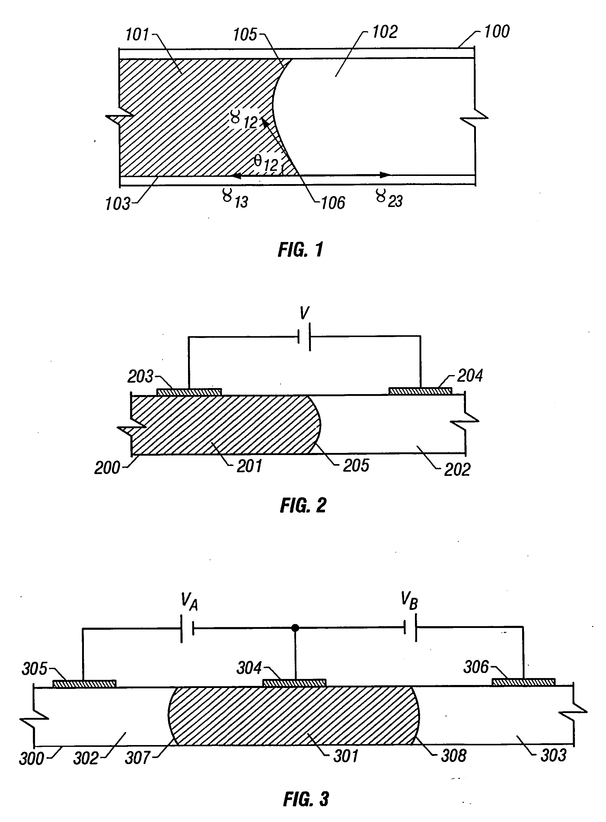
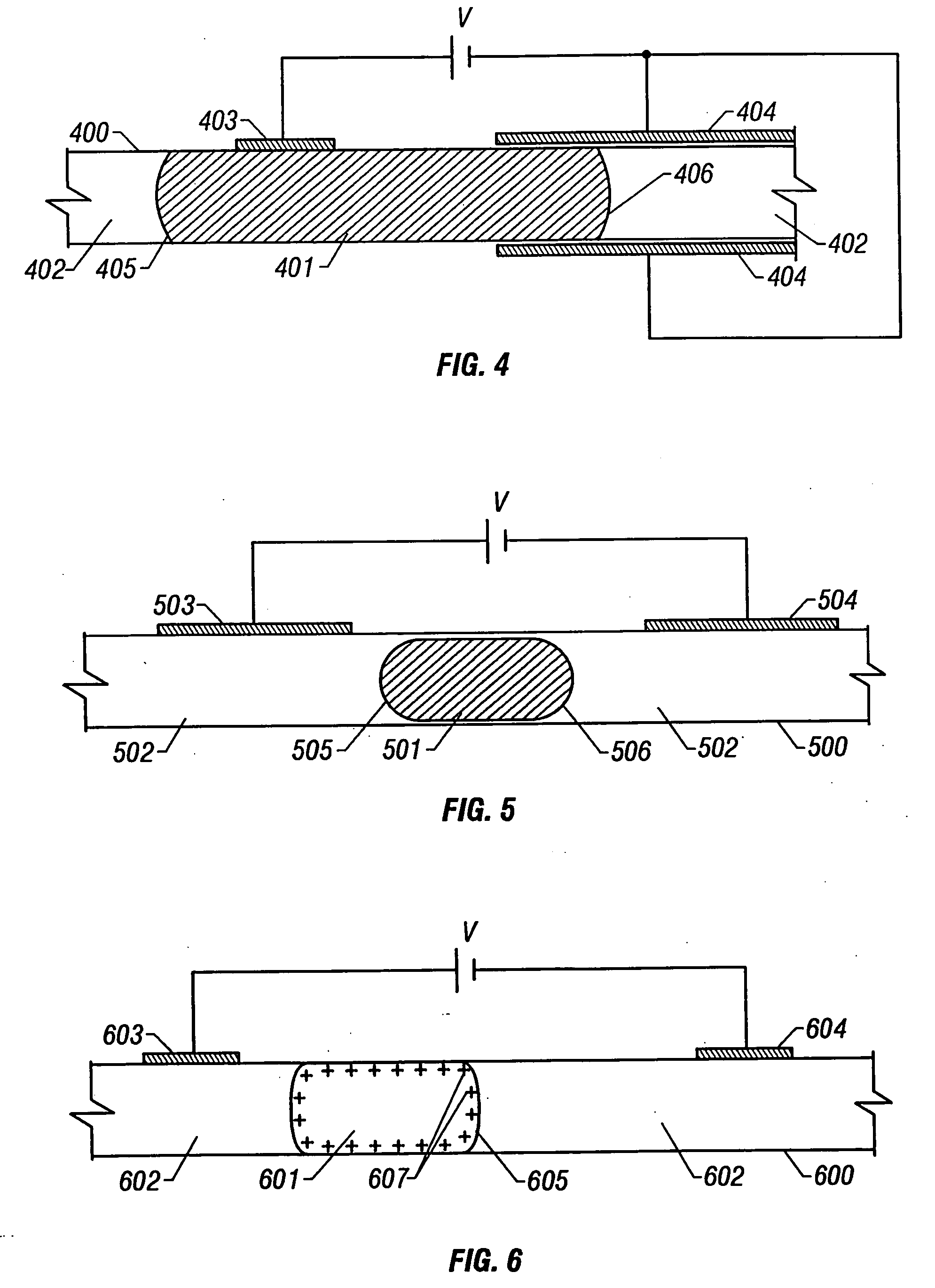
[0061] Several embodiments are discussed below and with reference to the attached drawings. These descriptions and drawings provide examples of certain embodiments of the invention and are not to be construed as limiting the scope of the invention. Instead, the invention is to be accorded the breadth as described herein and as defined in the claims that form part of this specification.

[0062] One factor in the operation of devices according to this invention is the ability to displace small volumes of liquid, in some cases only a few picoliters, in response to an electrical signal. Fluids can be moved by dielectric pumping or variable dielectric pumping, in which a difference in capacitance is used to move two dielectric fluids in contact with one another. Other forces used to move fluids include electrical effects (such as electrocapillarity, differential-pressure electrocapillarity, electrowetting, and continuous electrowetting) and thermal effects (such as thermocapillarity) that...


PUM


Abstract

Devices utilize elements carried by a fluid in a microchannel to switch, attenuate, shutter, filter, or phase shift optical signals. In certain embodiments, a microchannel carries a gaseous or liquid slug that interacts with at least a portion of the optical power of an optical signal traveling through a waveguide. The microchannel may form part of the cladding of the waveguide, part of the core and the cladding, or part of the core only. The microchannel may also have ends or may be configured as a loop or continuous channel. The fluid devices may be self-latching or may be semi-latching. The fluid in the microchannel is moved using e.g., e.g., electrocapillarity, differential-pressure electrocapillarity, electrowetting, continuous electrowetting, electrophoresis, electroosmosis, dielectrophoresis, electro-hydrodynamic electrohydrodynamic pumping, magneto-hydrodynamic magnetohydrodynamic pumping, thermocapillarity, thermal expansion, dielectric pumping, and / or variable dielectric pumping.

Description

[0001] This application is a divisional of U.S. patent application Ser. No. 10 / 085,885, filed Feb. 27, 2002, which claims the benefit of priority of U.S. Provisional Ser. No. 60 / 272,337, filed Feb. 28, 2001, the contents of which are hereby incorporated by reference into the present disclosure. This application also incorporates by reference U.S. Provisional Application Ser. No. 60 / 360,742, entitled “Microfludic Control For Waveguide Optical Switches, Variable Attenuators, And Other Optical Devices” filed on Feb. 27, 2002.TECHNICAL FIELD [0002] This invention relates generally to optical switches, shutters, and dynamically programmable optical attenuators. In particular, the invention provides implementations for switching optical signals among optical waveguides or changing the transmission of optical signals within optical waveguides by means of displacement of fluids incorporated within or adjoining to waveguide structures. Application of the invention facilitates the implementat...

Claims


Application Information

Patent Timeline
Patent Type & Authority Applications(United States)
IPC IPC(8): G02B6/10B01F13/00B01L3/00F04B19/00G02B6/35G02B26/02
CPCB01F13/0059B01F13/0076B01J2219/00274B01L3/50273B01L2300/0816B01L2400/0427B01L2400/086F04B19/006G02B6/3536G02B6/3538G02B6/3546G02B6/355G02B6/3552G02B6/3568G02B6/357G02B6/3574G02B6/3576G02B6/358G02B6/3594G02B26/005B01F33/3031B01F33/30
Inventor TICKNOR, ANTHONY J.KENNEY, JOHN T.VACCA, GIACOMOSAVILLE, DUDLEY A.PURCHASE, KEN G.
Owner NEOPHOTONICS CORP
Why Eureka
Try Eureka