Technique for optical inspection system verification

a technology of optical inspection system and optical inspection, applied in the direction of instruments, soldering apparatus, image enhancement, etc., can solve the problems of reducing accuracy, requiring costly and time-consuming pcb rework, and more than 60 percent of solder defects at the printing stage of solder pas

Inactive Publication Date: 2006-04-27
DELPHI TECH INC
View PDF10 Cites 29 Cited by
  • Summary
  • Abstract
  • Description
  • Claims
  • Application Information

AI Technical Summary

Benefits of technology

[0008] The present invention is directed to a technique for optical inspection verification that implements a number of steps. Initially, a simulated solder paste material including a solder powder and an organic resin, is provided. Next, the simulated solder paste material is printed in a desired pattern on a base material, e.g., a printed circuit board (PCB), to provide a reference test board. Then, the test board is cured to stabilize the simulated solder paste material. Next, the test board is ut

Problems solved by technology

According to another study, more than sixty percent of solder defects occur at the solder paste printing stage.
It should be appreciated that when soldering defects are not identified until after a PCB has been populated, costly and time-consuming rework of the PCB is required.
Further, as the majority of surface mount solder defects result from poor solder paste printing, inspection after solder paste printing offers considerable benefits.
However, this approach may miss flaws, such as dog ears and stencil blockages at the edges of a pad, and exhibit reduced accuracy and have limited repeatability.
While automated optical inspection (AOI) systems with optional 3D sensing capability can be utilized for inspection of solder paste, in practice, such systems have not traditionally been implemented.
Typically, solder paste print (deposit) defects can be attributed to stencil misalignment and excessive paste, which leads to bridging, shorts and tombstoning during the mou

Method used


Image

  • Technique for optical inspection system verification
  • Technique for optical inspection system verification

Examples


Embodiment Construction

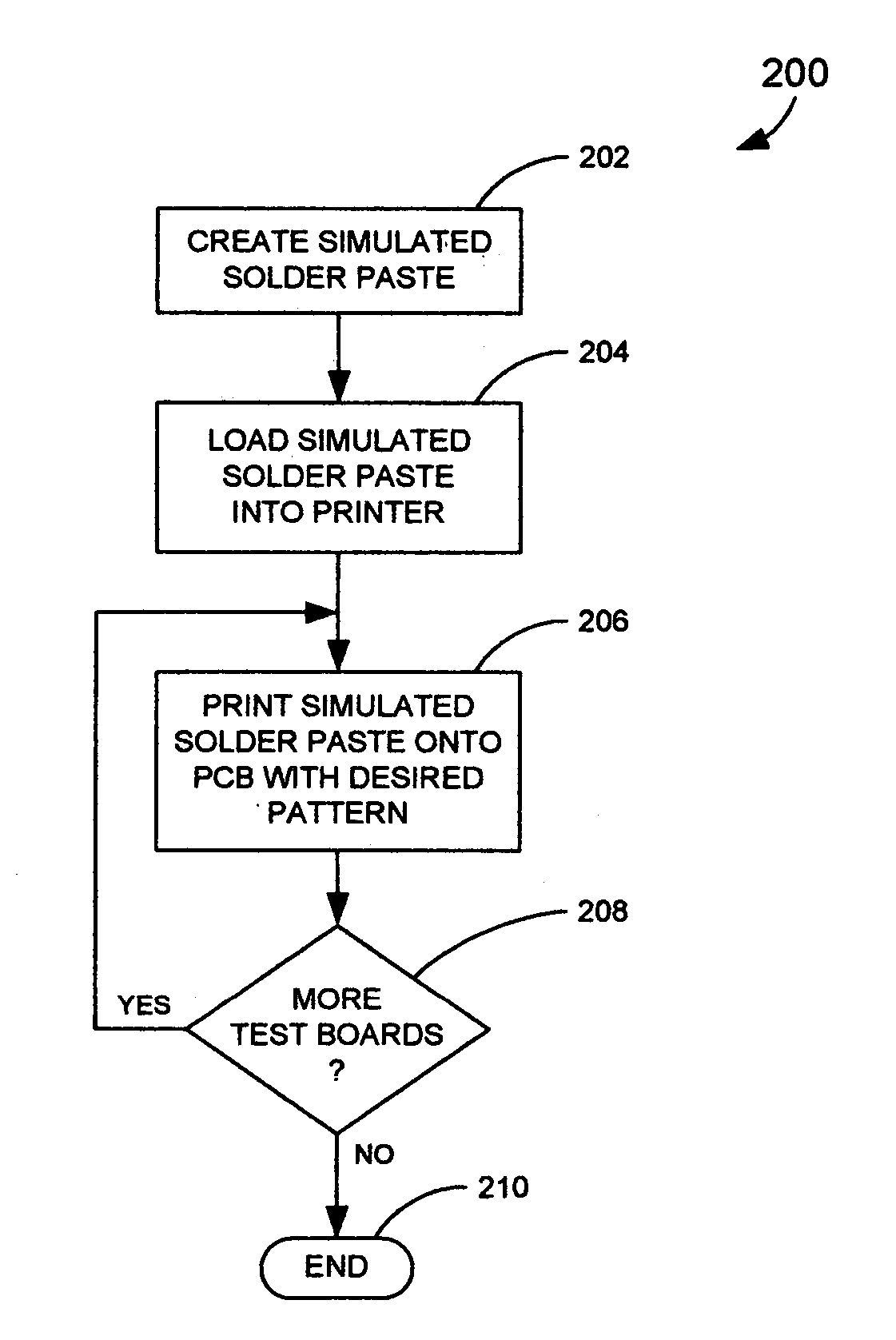
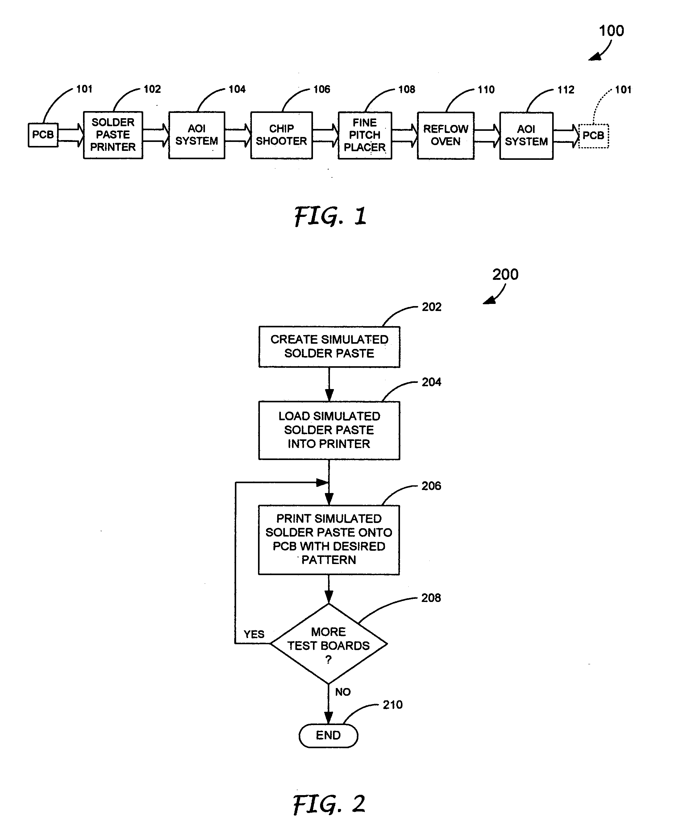
[0014] According to the present invention, a technique for optical inspection system verification utilizes a simulated solder paste, e.g., a solder powder and an organic resin, which is printed (or stenciled) like solder paste but cures and holds its shape. The simulated solder material is deposited on a base material, e.g., a production printed circuit board (PCB) or ceramic substrate or any substrate material (e.g., flex or laminate, such as FR-4, CEM-1, CEM-2, CEM-3, phenolics, BT and polyimides), and cured. The cured PCB (or reference test board) is then used to periodically verify proper operation of the inspection system. Multiple test boards may be created with some of the test boards having known defects, such as no paste, misregistered paste, smeared paste, excessive paste or insufficient paste. The defective reference test boards may then be used in conjunction with defect-free reference test boards to verify the inspection system is operating correctly. Further, the refer...


PUM

PropertyMeasurementUnit
Fractionaaaaaaaaaa
Fractionaaaaaaaaaa
Weightaaaaaaaaaa

Abstract

A technique for optical inspection verification implements a number of steps. Initially, a simulated solder paste material, including a solder powder and an organic resin, is provided. Next, the simulated solder paste material is printed in a desired pattern on a base material to provide a reference test board. Then, the test board is cured to stabilize the simulated solder paste material. Next, the test board is utilized to train the optical inspection system to reject defective product.

Description

TECHNICAL FIELD [0001] The present invention is generally directed to a technique for optical inspection system verification and, more specifically, to verifying proper operation of an optical inspection system that inspects solder paste deposited upon a printed circuit board. BACKGROUND OF THE INVENTION [0002] To date, the proliferation of hand-held and laptop electronic devices, e.g., pagers, cell phones and computers, have resulted in a need for relatively small printed circuit boards (PCBs) with reduced spacing between electronic components mounted to the PCBs. Various industry studies have indicated that approximately fifty percent of all electronics assembly errors and sixty-five percent of service mount technology (SMT) defects are related to solder paste printing and solder joint formation. These studies have generally confirmed that effective and thorough solder paste inspection, immediately after solder paste printing, is desirable to ensure high yields, minimize rework / re...

Claims


Application Information

Patent Timeline
IPC IPC(8): B23K1/00
CPCG01N21/95684G01R31/2812G01R31/309G06T7/0008G06T7/001G06T2207/30152H05K1/0269H05K3/3484H05K2201/10204H05K3/3485
Inventor SANFTLEBEN, HENRY M.HUTCHINS, REBECCA A.LAWRENCE, ERIN M.CHANDLER, BRIAN LEE
Owner DELPHI TECH INC
Why Eureka
Try Eureka