Solid-state imaging device

Active Publication Date: 2006-04-27
SONY SEMICON SOLUTIONS CORP
View PDF12 Cites 104 Cited by
  • Summary
  • Abstract
  • Description
  • Claims
  • Application Information

AI Technical Summary

Benefits of technology

[0013] There is a need for a backside-illumination-type solid-state imaging device which can prevent light that has entered from the backside of a substrate, has been transmitted through a p

Problems solved by technology

It is, however, difficult to allow a gate oxide film to function as a reflection film using a MOS process.
Such an approach is not disclosed in Patent Document

Method used


Image

  • Solid-state imaging device
  • Solid-state imaging device
  • Solid-state imaging device

Examples


example 1

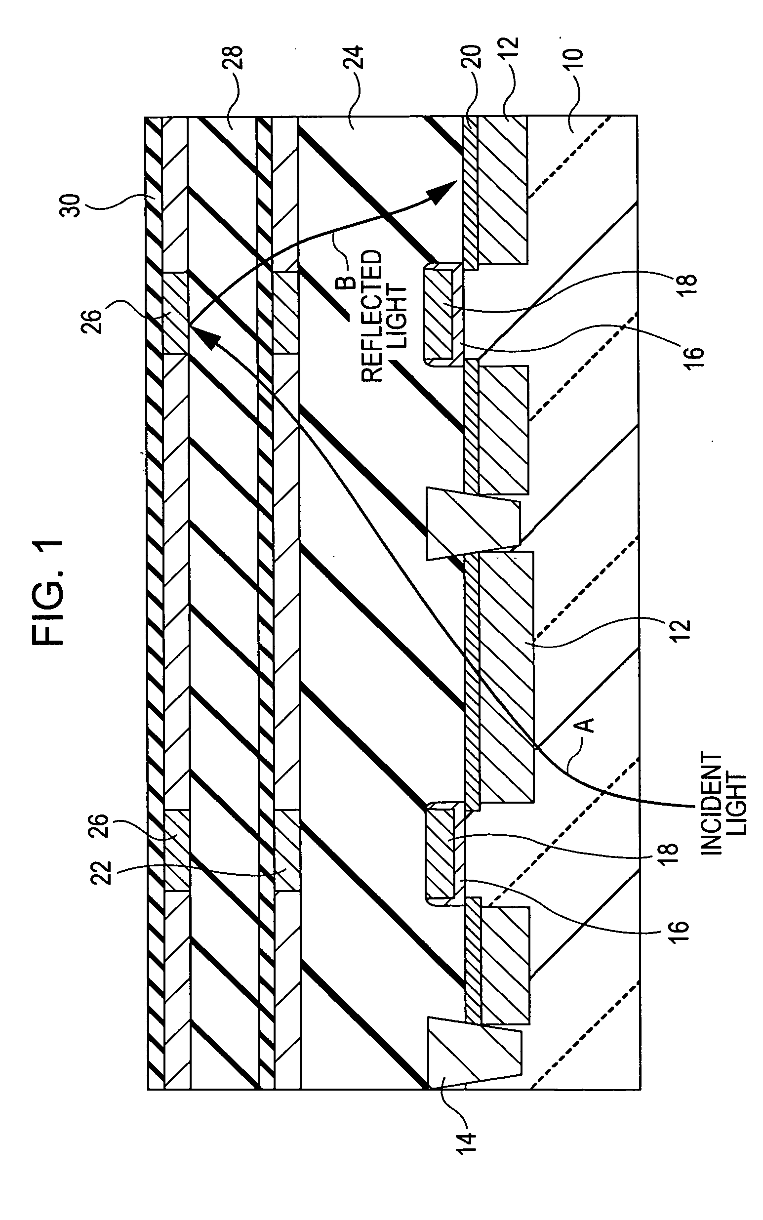
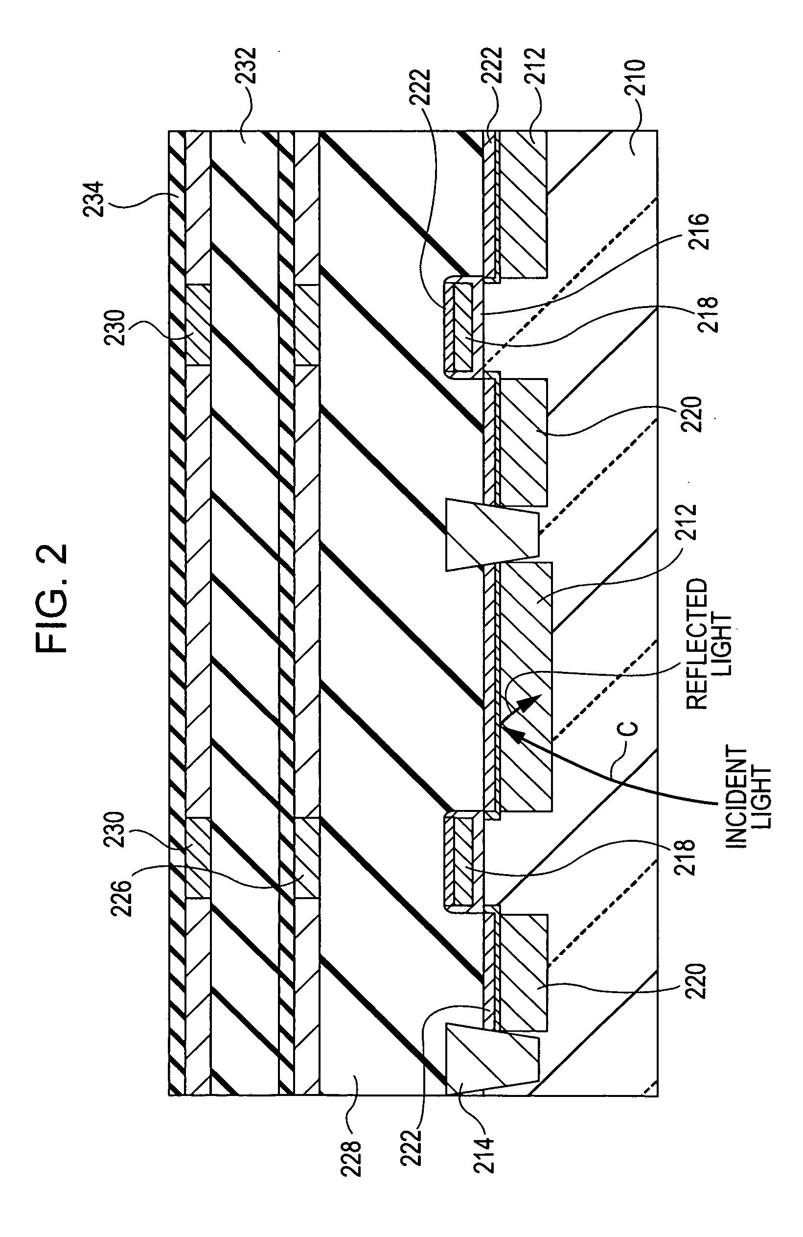
[0032]FIG. 2 is a cross-sectional view showing an example of a structure of a solid-state imaging device according to Example 1 of the present invention, and FIG. 3 is a circuit diagram showing an example of a configuration of a circuit region (pixel transistor circuit) in the solid-state imaging device shown in FIG. 2. FIGS. 4 to 12 are cross-sectional views each showing a specific example of a method for fabricating the solid-state imaging device shown in FIG. 2.

[0033] First, as shown in FIG. 3, in the solid-state imaging device according to this example, each pixel is provided with a photodiode (PD) 100 functioning as a photoelectric conversion section, a reset transistor 110 for resetting charges accumulated in the photodiode 100, an amplifier transistor 120 for amplifying and outputting pixel signals corresponding to the amount of accumulated charges, a transfer transistor 130 for selecting the timing of transfer of signal charges accumulated in the photodiode 100 to the gate ...

example 2

[0043]FIG. 13 is a cross-sectional view showing an example of a structure of a solid-state imaging device according to Example 2 of the present invention. The same reference numerals are used to designate the same elements as those shown in FIG. 2.

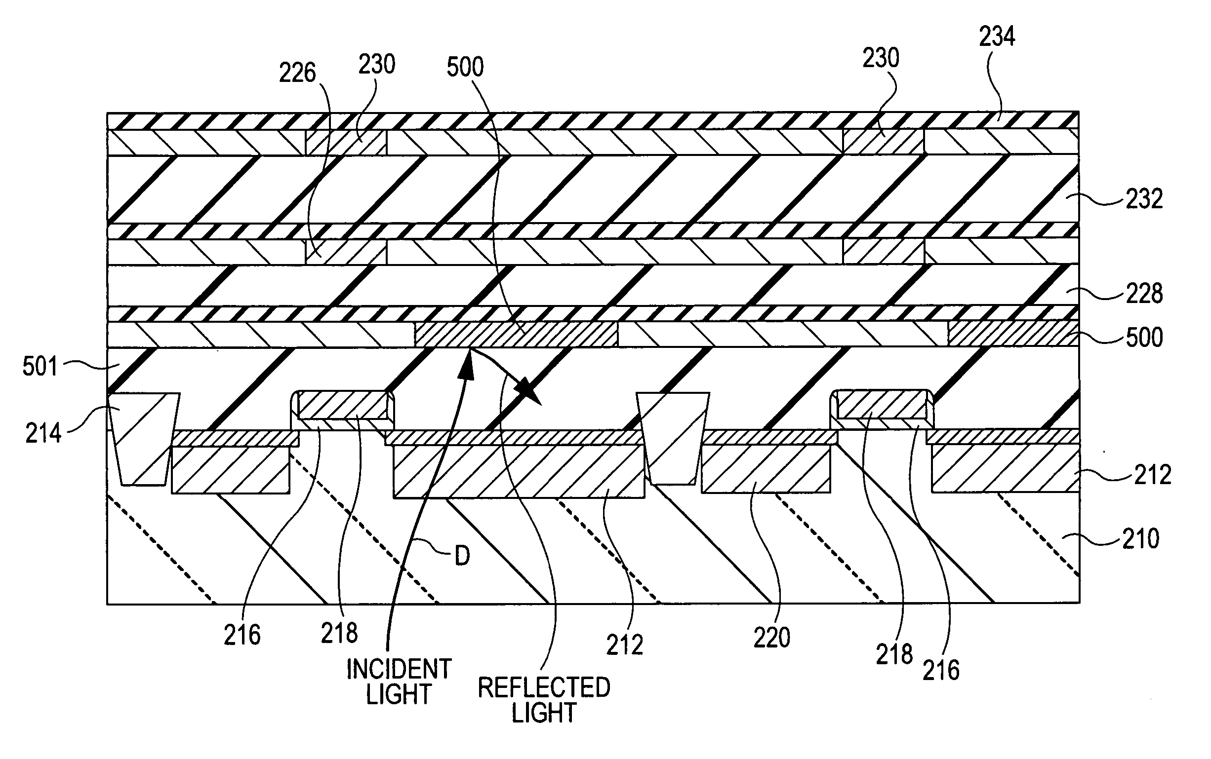
[0044] In Example 2, in place of the silicide films described above, light-shielding dummy wiring films 500 are disposed as films that prevent transmission of light.

[0045] As shown in FIG. 13, the light-shielding dummy wiring films 500 are disposed in the lowest layer under the layers in which wiring films having the original function are disposed. An interlayer insulating film 501 is disposed thereunder. The dummy wiring films 500 are not composed of a material that transmits light, such as polysilicon, but are composed of a metal, such as tungsten or aluminum, or composed of an alloy. As shown in FIG. 13, the dummy wiring films 500 are formed in a pattern corresponding to light-receiving regions of the photodiodes. In Example 2, as ind...

example 3

[0046]FIG. 14 is a cross-sectional view showing an example of a structure of a solid-state imaging device according to Example 3 of the present invention. The same reference numerals are used to designate the same elements as those shown in FIG. 2.

[0047] In Example 3, as films that prevent transmission of light, interlayer films having a light-absorbing property are used.

[0048] As shown in FIG. 14, interlayer insulating films 510 and 520 are disposed between the silicon substrate and a first wiring film layer and between the first wiring film layer and a second wiring film layer, respectively. These interlayer insulating films 510 and 520 serve as light-absorbing films. Specifically, for example, silicon carbide (SiC) may be used.

[0049] By providing such interlayer insulating films 510 and 520, as indicated by an arrow E in FIG. 14, even if light that has entered from the backside reaches the front side of the substrate, light is absorbed by the interlayer insulating films 510 an...


PUM


Abstract

A solid-state imaging device includes a photoelectric conversion section which is provided for each pixel and which converts light incident on a first surface of a substrate into signal charges, a circuit region which reads signal charges accumulated by the photoelectric conversion section, a multilayer film including an insulating film and a wiring film, the multilayer film being disposed on a second surface of the substrate opposite to the first surface, and a transmission-preventing film disposed at least between the wiring film in the multilayer film and the substrate.

Description

CROSS REFERENCES TO RELATED APPLICATIONS [0001] The present invention contains subject matter related to Japanese Patent Application JP 2004-306182 filed in the Japanese Patent Office on Oct. 20, 2004, the entire contents of which are incorporated herein by reference. BACKGROUND OF THE INVENTION [0002] 1. Field of the Invention [0003] The present invention relates to a backside-illumination-type solid-state imaging device in which a light-receiving surface of a photoelectric conversion section is disposed on a backside of a substrate. In particular, the invention relates to a solid-state imaging device that is suitable for use in CMOS image sensors manufactured using a MOS process. [0004] 2. Description of the Related Art [0005] Recently, in solid-state imaging devices, such as CCD image sensors and CMOS image sensors, with the reduction in the size of devices to be mounted, the chip area has been reduced and reduction in the area per pixel has been necessitated. As a result, in a s...

Claims


Application Information

Patent Timeline
IPC IPC(8): H01L31/113H01L27/14H01L27/146H01L31/10H04N5/335H04N5/369H04N5/374
CPCH01L27/14603H01L27/1462H01L27/14623H01L27/1464H01L27/14632H01L27/14629H01L27/14625H01L27/146
Inventor FURUKAWA, MASAKAZUMABUCHI, KEIJI
Owner SONY SEMICON SOLUTIONS CORP
Why Eureka
Try Eureka