

Solid state imaging device
- Summary
- Abstract
- Description
- Claims
- Application Information
AI Technical Summary
Benefits of technology
Problems solved by technology
Method used
Image

Examples
first embodiment
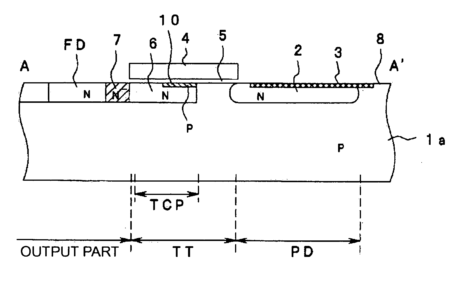
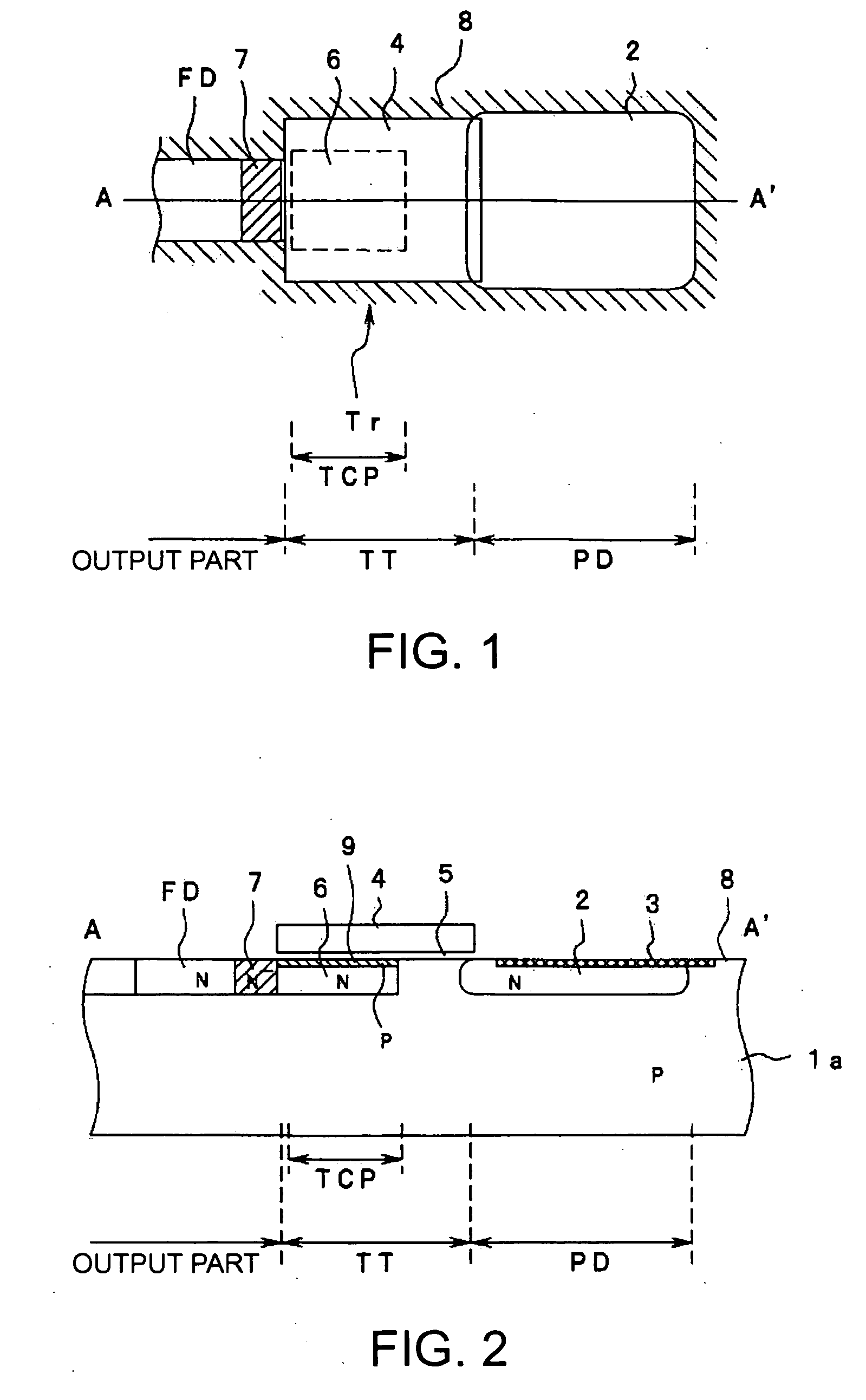
[0027] Embodiments of the invention will now be described with reference to the drawings. FIG. 1 is a plan view of a solid-state imaging device according to the invention showing its planar shape. FIG. 2 is a sectional view along the line A-A′ in FIG. 1
[0028] The solid-state imaging device of this embodiment has a sensor cell array having a plurality of sensor cells arranged in a two-dimensional matrix on a substrate surface. FIG. 1 only shows a single sensor cell placed in the middle of the sensor cell array. Each sensor cell has the same structure. Each sensor cell includes a photodiode, a transfer part and an output part. The photodiode generates the photo-generated electric charges according to an incident light. The transfer part transfers the photo-generated electric charges generated by the photodiode. The output part includes the floating diffusion that stores the photo-generated electric charges transferred by the transfer part. The output part outputs an electric potential...
second embodiment
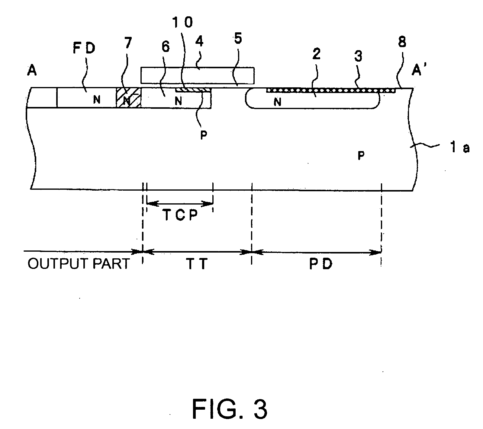
[0046]FIG. 3 is a sectional view showing the invention. In FIG. 3, the identical numerals are given to the same structures as those in FIG. 2 and those explanations will be omitted.
[0047] The first embodiment is for preventing the generation of the dark current. The second embodiment is for reducing the electric charges left without being transferred. The second embodiment is different from the first embodiment in that a buried layer 10 is used instead of the buried layer 9.
[0048] The buried layer 10 is the P-type impurity layer and formed on the photodiode forming region PD side of the substrate surface that contacts with the gate insulating layer 5 in the transfer part forming region TT. This means that at least a part of the top surface of the N-type impurity layer 6, which is the charge retention region, is covered with the P-type impurity layer 10 which is the buried layer. In other words, the impurity layer 6 does not contact with the gate insulating layer 5 in the area where...
PUM
 Abstract
Description
Claims
Application Information