

Method of successively depositing multi-film releasing plasma charge
- Summary
- Abstract
- Description
- Claims
- Application Information
AI Technical Summary
Benefits of technology
Problems solved by technology
Method used
Image

Examples
Embodiment Construction
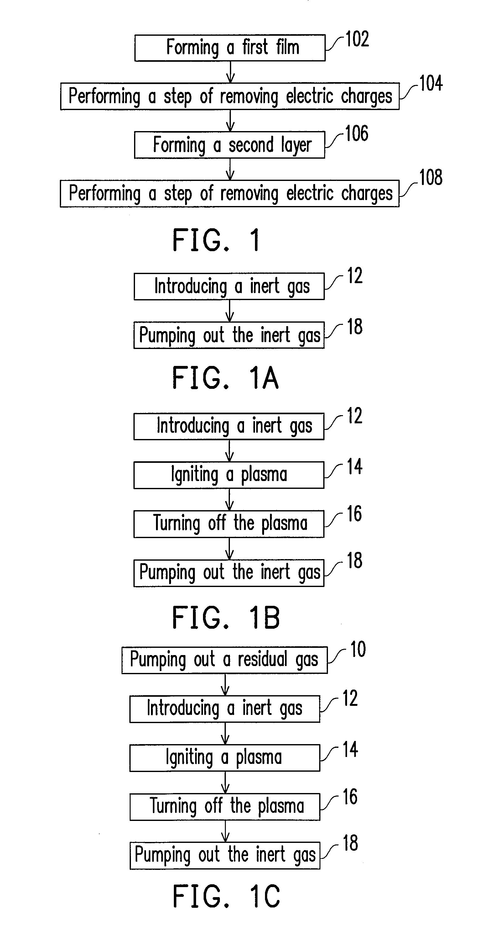
[0039]The method of depositing the multi-film according to the present invention is to perform a step of removing the electric charges after the deposition of the last film and / or between the two adjacent film deposition processes, so that the electric charges accumulated on the substrate are removed and thereby reduced. Details are illustrated below.
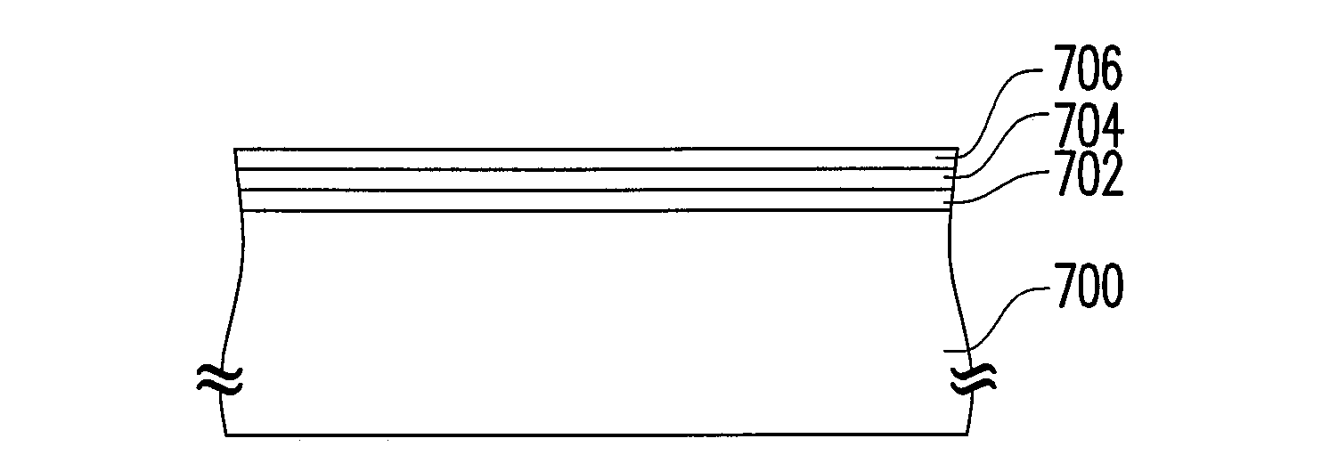
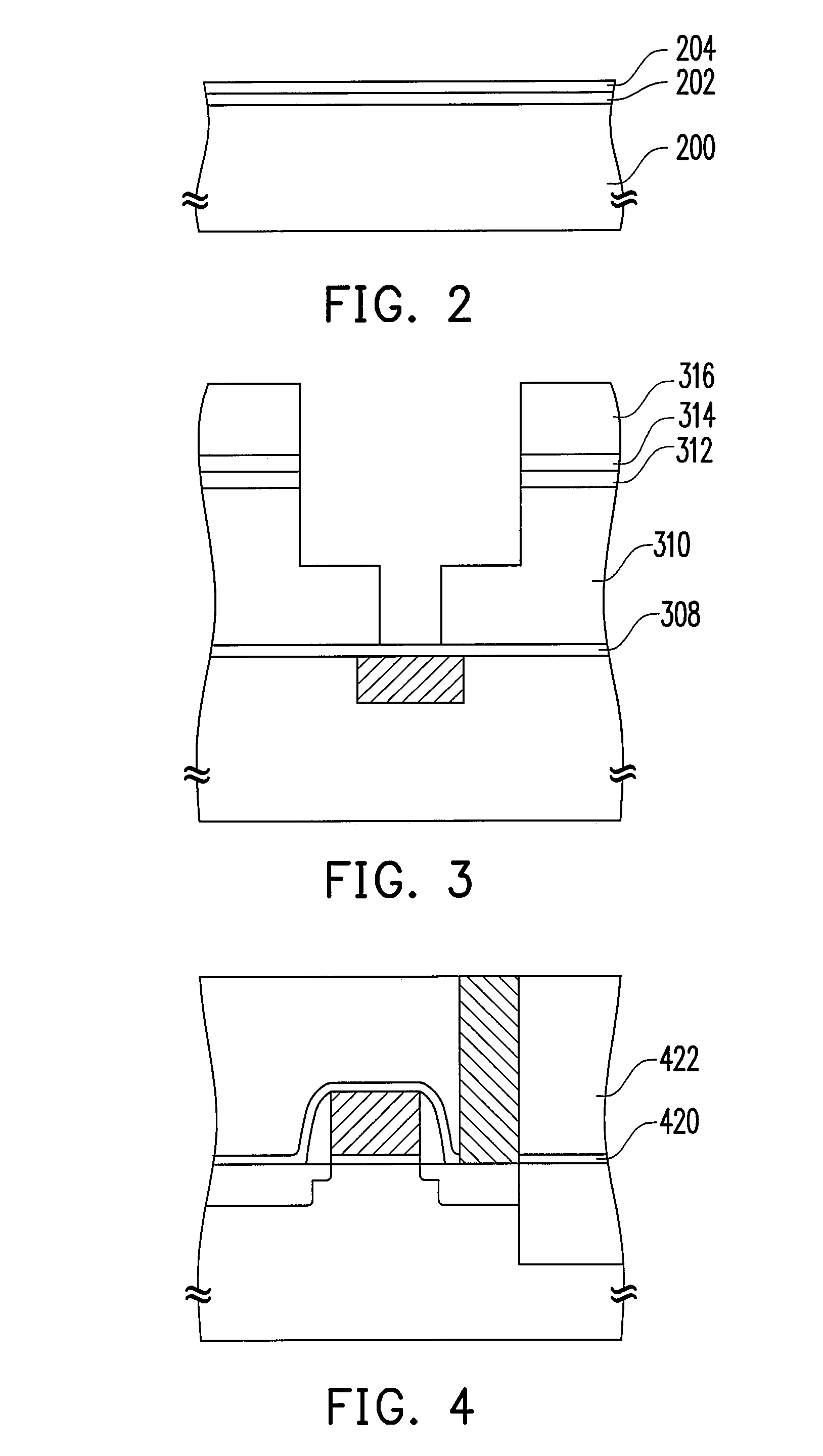
[0040]FIG. 1 is a flow diagram showing a method of a plasma chemical vapor deposition system to successively deposit double-stacked film, according to one embodiment of the present invention. FIG. 2 is a schematic cross-sectional view showing a substrate having a double-stacked film, according to one embodiment of the present invention.
[0041]Referring to FIGS. 1 and 2, Step 102 is performed by forming a first film 202 on a substrate 200. The method of the process is to introduce reaction gas and carrier gas to the reaction chamber of the Plasma Enhanced chemical vapor deposition system or the High Density Plasma Deposition System. After...
PUM
| Property | Measurement | Unit |
|---|---|---|
| Time | aaaaa | aaaaa |
| Power | aaaaa | aaaaa |
| Power | aaaaa | aaaaa |
Abstract
Description
Claims
Application Information