
Delay stage-interweaved analog DLL/PLL

a delay stage and analog technology, applied in the field of memory systems, can solve the problems of increasing the corresponding overall delay, vcdl may not properly function at low input clock frequency, and it is not possible to obtain a delay range of 1 ns, so as to achieve a wide frequency range of operation, reduce current consumption, and fast lock time

Active Publication Date: 2006-04-27
MICRON TECH INC
View PDF11 Cites 10 Cited by
  • Summary
  • Abstract
  • Description
  • Claims
  • Application Information

AI Technical Summary

Benefits of technology

The present patent text discusses an improved analog delay locked loop (ADLL) that can program delay stages based on the operating condition, such as the frequency of the reference clock. This results in faster locking time, a wider frequency range of operation, and lower current consumption at high frequencies. The number of delay stages can be flexibly set based on the input clock frequency, and unused delay stages can be deactivated to conserve power. The technical effects of this invention include improved performance, flexibility, and efficiency in analog delay locked loops.

Problems solved by technology

At high reference clock frequencies, it may not be preferable to increase the number of VCDL stages because that may also increase the corresponding overall delay.
However, on the other hand, if less than optimum number of VCDL stages are employed, the VCDL may not properly function at low input clock frequencies.
However, with the same number (4) of VCDL stages, it may not be possible to obtain a delay range of 1 ns-4 ns which may be needed to accommodate a higher reference clock frequency (e.g., a frequency having a clock period tCK=1 ns).
The inventors have recognized that the frequency range of operation, locking time, and current consumption (e.g., at higher frequencies) of a prior art analog delay locked loop may be negatively affected because of the usage of all delay line stages for all frequencies of operation.
This arrangement not only consumes extra current (and, hence, power) at higher frequencies of operation, but also results in inefficient and inflexible usage of the delay line.
The usage of the entire delay line for each frequency delay operation results in slower locking time and a narrow frequency range of operation.

Method used


Image

  • Delay stage-interweaved analog DLL/PLL
  • Delay stage-interweaved analog DLL/PLL
  • Delay stage-interweaved analog DLL/PLL

Examples


Embodiment Construction

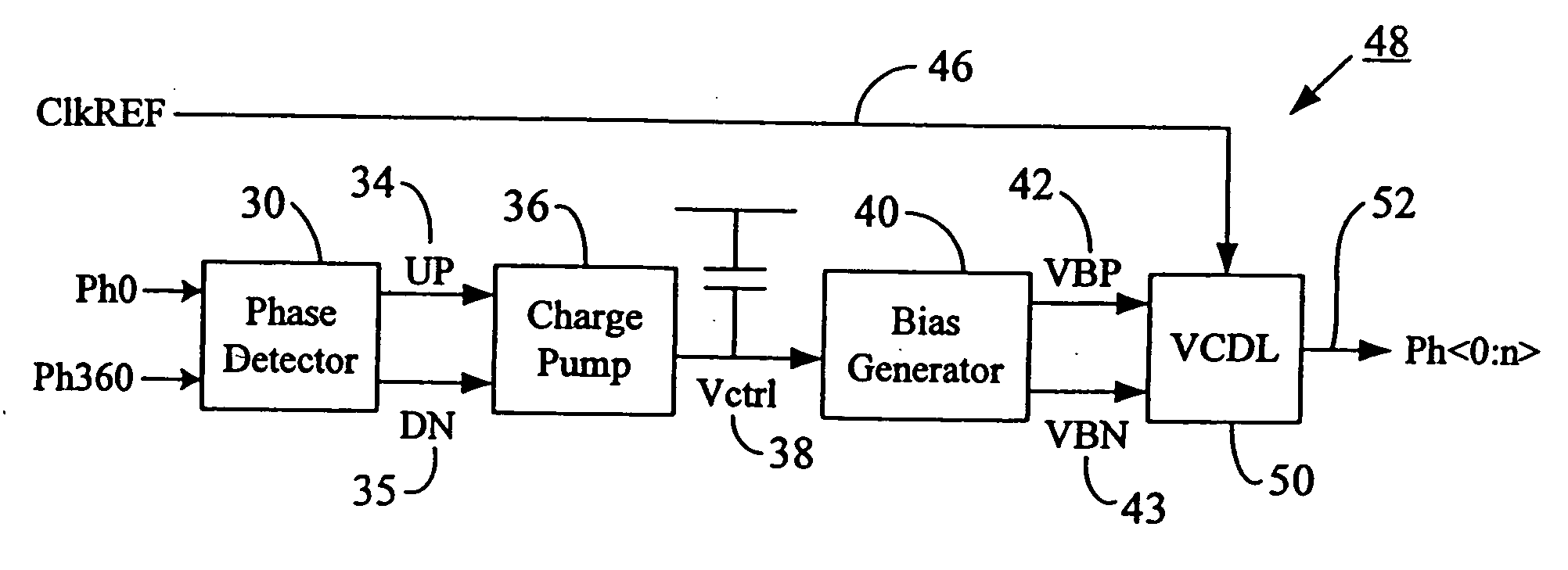
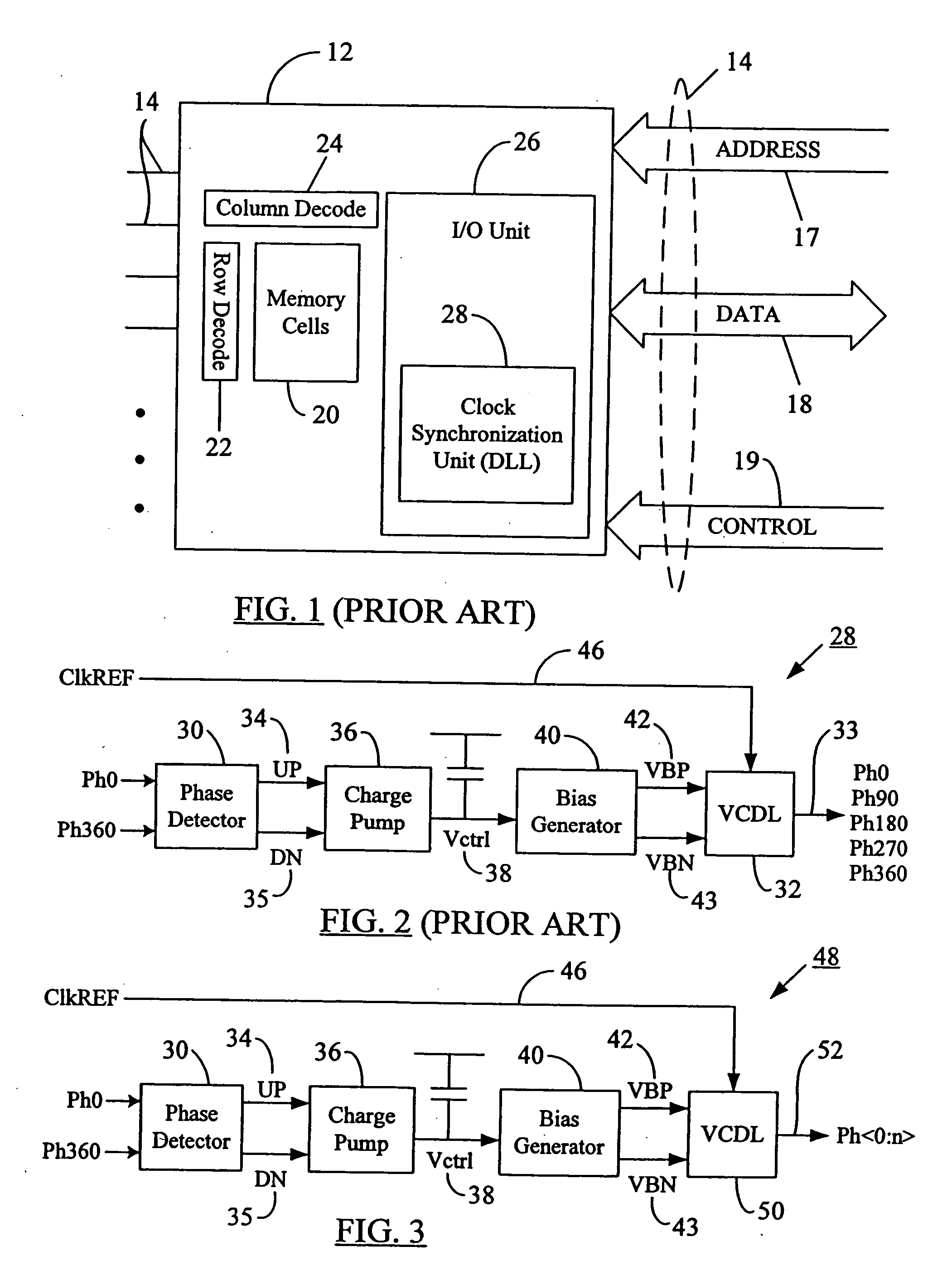
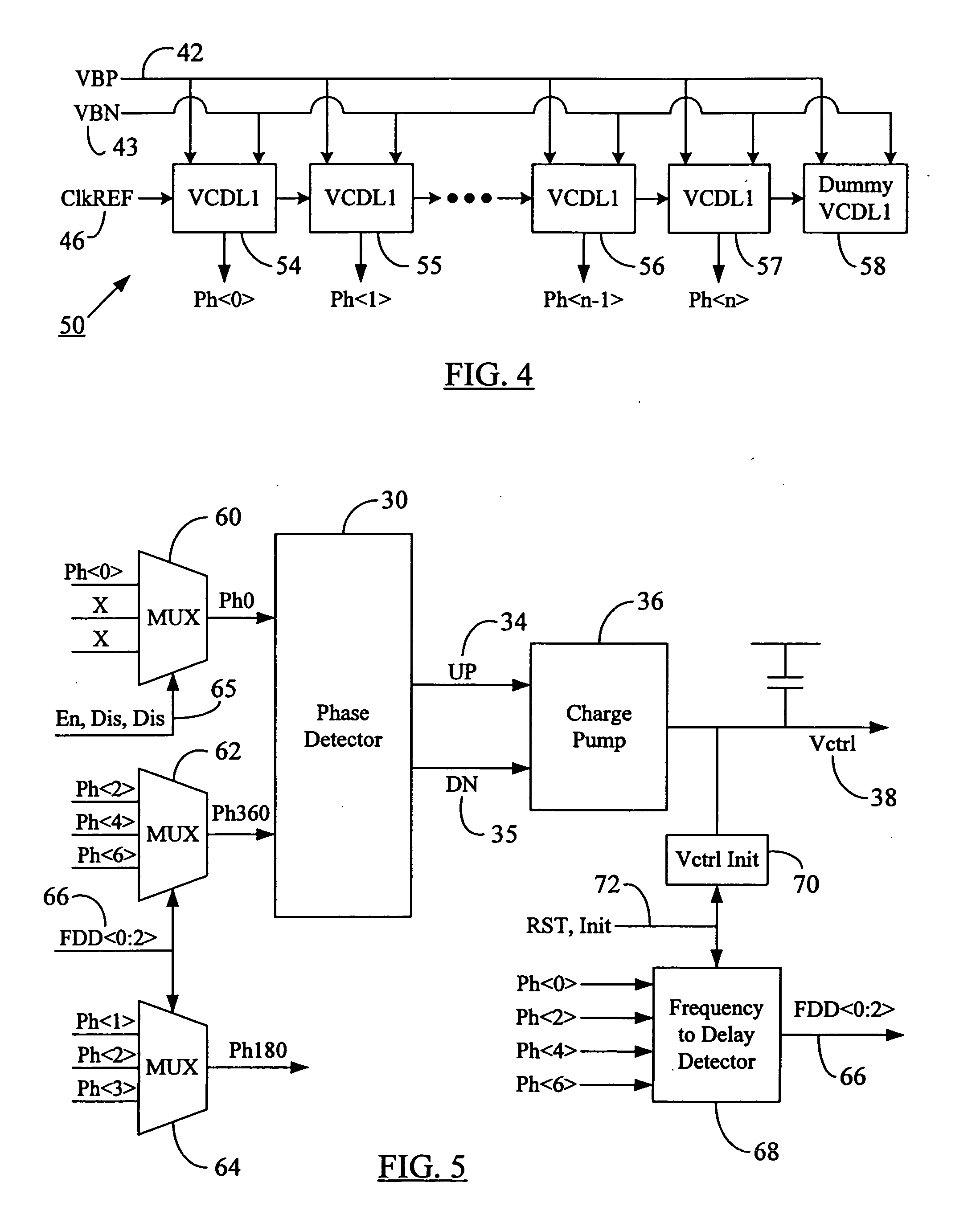
[0038] Reference will now be made in detail to certain embodiments of the present disclosure, examples of which are illustrated in the accompanying figures. It is to be understood that the figures and descriptions of the present disclosure included herein illustrate and describe elements that are of particular relevance to the present disclosure, while eliminating, for the sake of clarity, other elements found in typical data storage or memory systems. It is noted at the outset that the terms “connected”, “connecting,”“electrically connected,” etc., are used interchangeably herein to generally refer to the condition of being electrically connected. It is further noted that various block diagrams, circuit diagrams and timing waveforms shown and discussed herein employ logic circuits that implement positive logic, i.e., a high value on a signal is treated as a logic “1” whereas a low value is treated as a logic “0.” However, any of the circuit discussed herein may be easily implemente...


PUM


Abstract

A methodology is disclosed that enables the delay stages of an analog delay locked loop (DLL) or phase locked loop (PLL) to be programmed according to the operating condition, which may depend on the frequency of the input reference clock. The resulting optimized delay stages allow for a broad frequency range of operation, fast locking time over a wide range of input clock frequencies, and a lower current consumption at high clock frequencies. Better performance is achieved by allowing the number of analog delay stages active during a given operation to be flexibly set. The deactivation or turning off of unused delay stages conserves power at higher frequencies. The high frequency range of operation is increased by using a flexible number of delay stages for various input clock frequencies. Because of the rules governing abstracts, this abstract should not be used to construe the claims.

Description

CROSS-REFERENCE TO RELATED APPLICATIONS [0001] This application is a divisional of U.S. application Ser. No. 10 / 893,804 entitled Delay Stage-Interweaved Analog DLL / PLL filed Jul. 19, 2004BACKGROUND [0002] 1. Field of the Disclosure [0003] The present disclosure generally relates to memory systems and, more particularly, to an analog delay locked loop (DLL) or phase locked loop (PLL) with delay stage interweaving. [0004] 2. Brief Description of Related Art [0005] Most digital logic implemented on integrated circuits is clocked synchronous sequential logic. In electronic devices such as synchronous dynamic random access memory circuits (SDRAMs), microprocessors, digital signal processors, etc., the processing, storage, and retrieval of information is coordinated or synchronized with a clock signal. The speed and stability of the clock signal determines to a large extent the data rate at which a circuit can function. Many high speed integrated circuit devices, such as SDRAMs, microproc...

Claims


Application Information

Patent Timeline
Patent Type & Authority Applications(United States)
IPC IPC(8): G08B13/14
CPCH03L7/0812H03L7/0814H03L7/0891H03L7/10G11C7/22G11C7/222G11C29/02G11C29/028G11C29/50012G11C2207/2254H03L7/0802H03L7/104
Inventor KIM, KANG YONGCHOI, DONG MYUNG
Owner MICRON TECH INC
Learn More