Semiconductor device

Inactive Publication Date: 2011-03-10
EPISIL TECH
View PDF2 Cites 34 Cited by
  • Summary
  • Abstract
  • Description
  • Claims
  • Application Information

AI Technical Summary

Benefits of technology

[0007]One embodiment of the invention provides a semiconductor device capable of being operated at the high voltage without

Problems solved by technology

Semiconductor design has to be improved along with increasing integration and increasing complicated requiremen

Method used


Image

  • Semiconductor device
  • Semiconductor device
  • Semiconductor device

Examples


Embodiment Construction

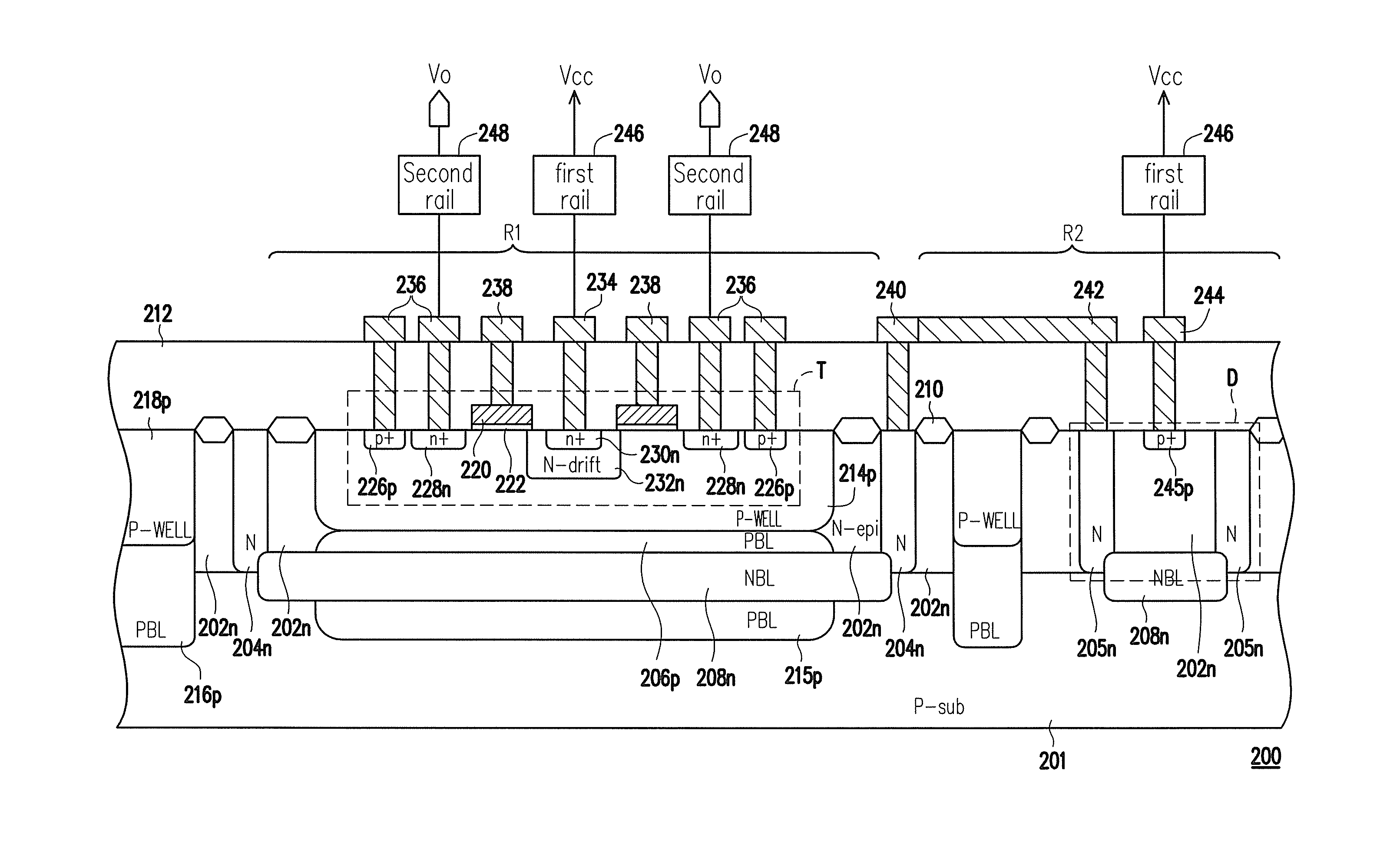
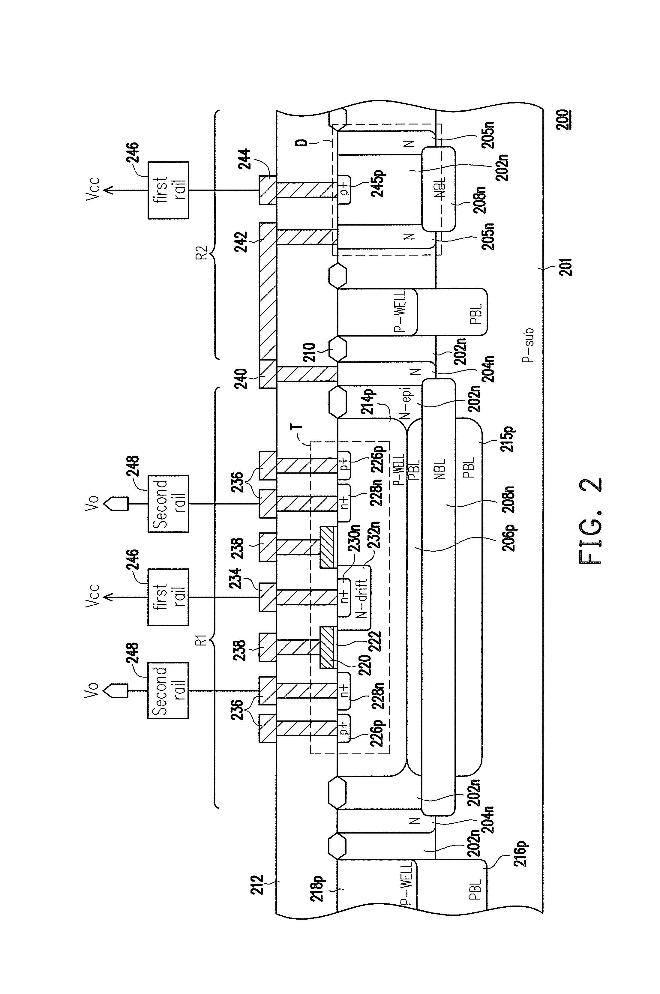
[0017]FIG. 2 is a cross-sectional view of a semiconductor device according to an embodiment consistent with the invention. Referring to FIG. 2, in the invention, the semiconductor device 200 includes a substrate 201, an epitaxial layer 202n, a first sinker 204n, a transistor T, a diode unit D, a first buried layer 206p and a second buried layer 208n. Moreover, the semiconductor device 200 further includes an isolation structure 210, a dielectric layer 212, a well region 214p, a buried layer 216p, a well region 218p, interconnects 234, 236, 238, 240, 242, and 244, but the invention is not limited to the particular embodiment disclosed herein.

[0018]In the present embodiment, the transistor T, for example, is a high voltage n-type metal-oxide-semiconductor (HV-NMOS), wherein a drain 230n thereof is electrically connected to a first rail 246, and a source 228n thereof is electrically connected to a second rail 248. Accordingly, when the semiconductor device 200 is applied to a switch de...


PUM


Abstract

A semiconductor device including a substrate, an epitaxial layer, a first sinker, a transistor, a diode unit, a first buried layer, and a second buried layer is provided. When the semiconductor device is operated at the high voltage, the highly large substrate current due to the external load is avoided through the diode unit disposed in the semiconductor device of an embodiment consistent with the invention. Furthermore, according to the design of the semiconductor device, the issue of the narrow input voltage range is improved, and interference of the semiconductor device with the other semiconductor devices is prevented.

Description

BACKGROUND OF THE INVENTION[0001]1. Field of the Invention[0002]The invention generally relates to a semiconductor device, and more particularly, to a semiconductor device capable of being operated at a high voltage without a large substrate current.[0003]2. Description of Related Art[0004]Semiconductor design has to be improved along with increasing integration and increasing complicated requirements thereof. For example, the design of high voltage devices must enable the high voltage devices to operate at a high voltage without effecting operation of other devices as well as large substrate currents.[0005]FIG. 1 is a schematic view of a switch device formed by two high voltage n-type metal-oxide-semiconductors (HV-NMOS). Referring to FIG. 1A, the switch device 10 includes a high-side HV-NMOS 12 and a low-side HVNMOS 14, wherein a drain of the high-side HV-NMOS 12 is electrically connected to a system power Vcc, and a source of the high-side HV-NMOS 12 is electrically connected to ...

Claims


Application Information

Patent Timeline
IPC IPC(8): H01L27/06
CPCH01L21/823425H01L27/0629H01L21/823493H01L29/7835
Inventor MA, SHIH-KUEIKUO, TA-CHUAN
Owner EPISIL TECH
Why Eureka
Try Eureka