Chip part manufacturing method and chip parts

a manufacturing method and chip technology, applied in the field of chip parts, can solve the problems of parts not being smoothly fed, broken or cracked chips, etc., and achieve the effects of suppressing chip rising, smooth feeding, and suppressing chip break or cracking

a manufacturing method and chip technology, applied in the field of chip parts, can solve the problems of parts not being smoothly fed, broken or cracked chips, etc., and achieve the effects of suppressing chip rising, smooth feeding, and suppressing chip break or cracking

US20060091534A1Inactive Publication Date: 2006-05-04PANASONIC CORP

Image

  • Chip part manufacturing method and chip parts
  • Chip part manufacturing method and chip parts
  • Chip part manufacturing method and chip parts

Examples


embodiment 1

Preferred Embodiment 1

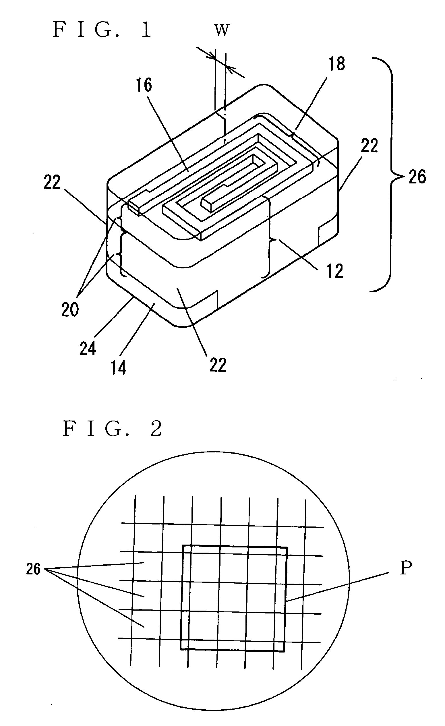
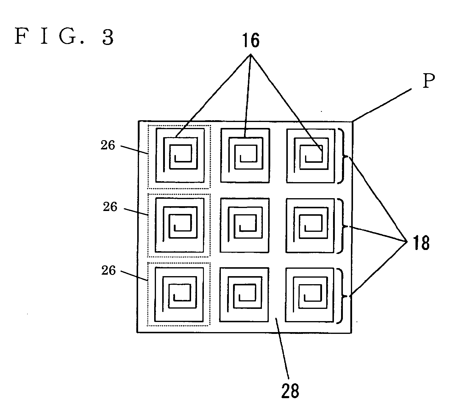
[0047]FIG. 1 is a perspective view of a chip part in the preferred embodiment 1. FIG. 2 is a plan view showing a state of a plurality of chip parts connected to each other. FIG. 3 is an enlarged view of portion P in FIG. 2. FIG. 4A to FIG. 4F are process diagrams showing a chip parts manufacturing process of the present invention.

[0048] In FIG. 1, chip part 26 in one preferred embodiment of the present invention is shown, for example, as a chip coil part. Chip part 26 comprises element 12 which is generally squared and transparent, electrode 14 disposed at the bottom of element 12, and coil section 18 formed by spiral metal layer 16 buried in element 12. Element 12 is formed by laminating insulating resin layers 20 formed from a photosensitive resin material obtained by hardening photosensitive resin.

[0049] Also, first corner 22 of chip part 26 is generally arcuate, which is formed at element 12, in a position perpendicular to the mounting surface. Second cor...

embodiment 2

Preferred Embodiment 2

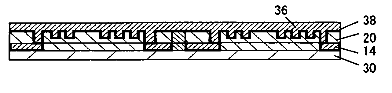
[0077]FIG. 5A to FIG. 5G show another manufacturing process of chip part 26 of the present invention. Since FIG. 1, FIG. 2 and FIG. 3 used in the preferred embodiment 1 can be used in the preferred embodiment 2 as well, the detailed description is omitted. As compared with the preferred embodiment 1, one more manufacturing process is shown in the preferred embodiment 2. Also, it is clear at first sight that FIG. 5A to FIG. 5G are similar to FIG. 4A to FIG. 4F.

[0078]FIG. 5A shows a step of forming an electrode. At the top of FIG. 5A, a release layer (not shown) is formed on one main surface of substrate 30, and insulating resin layer 20 having electrode void portion 34 is formed by a photolithography process on the upper surface of the release layer. The release layer can be, for example, formed by using release resist. In the case of forming a release layer, the chip parts described later can be easily separated from the frame-like connection and it is possibl...


PUM


Abstract

The present invention provides a chip part manufacturing method comprising a separating process capable of suppressing deformation of chip parts, and also provides chip parts. It comprises a step of forming a plurality of frame-like void portions (32) in one main surface of substrate (30) and insulating resin layer (20) having a spiral void portion (40) disposed in the region thereof, a step of forming metal layer (36) in frame-like void portion (32) and spiral void portion (40) and on insulating resin layer (20), a step of polishing metal layer (36) at least up to the upper surface of insulating resin layer and forming coil section (18) in spiral void portion (40), and a step of forming a metal layer for connecting chip parts to frame-like void portion (32), wherein the metal layer is melted and removed by using an etching agent to separate a plurality of chip parts connected to each other by a frame-like connection.

Description

TECHNICAL FIELD [0001] The present invention relates to a method of manufacturing chip parts used in various electronic apparatuses, and chip parts. BACKGROUND ART [0002]FIG. 6A to FIG. 6D are process diagrams showing a conventional chip part manufacturing process. FIG. 7 is an exploded perspective view of portion S of the chip part in FIG. 6B. [0003]FIG. 6A is a sheet forming diagram, FIG. 6B is a coil section forming diagram, FIG. 6C is an element separating diagram, and FIG. 6D is an electrode forming diagram, which respectively show the manufacturing processes. [0004] As shown in FIG. 6A, in the sheet forming process, a plurality of green sheets 1 are formed. Subsequently, as shown in FIG. 6B and in FIG. 7 mentioned later, in the coil forming process, arcuate conductors 2 are printed on the plurality of green sheets 1 by using Ag paste. Next, green sheets 1 are laminated to form coil section 3 formed from spiral conductor. In this case, arcuate conductors 2 printed on respective...

Claims


Application Information

Patent Timeline
04 May 2006
Publication
US20060091534A1
IPC
H01L23/34; H01L23/544
CPC
H01F17/0013; H01F41/041; H05K3/002; H05K3/0052; H05K3/045; H05K3/06; H05K3/107; H05K3/108
Inventors
OHBA, MITIO; MATSUTANI, NOBUYA