

Method and apparatus for variable polarization control in a lithography system
a lithography system and variable polarization technology, applied in the field of lithography systems, can solve the problem that the capacity of the process will be limited by the available level of imaging accuracy, and achieve the effect of increasing optical efficiency
- Summary
- Abstract
- Description
- Claims
- Application Information
AI Technical Summary
Benefits of technology
Problems solved by technology
Method used
Image

Examples
Embodiment Construction
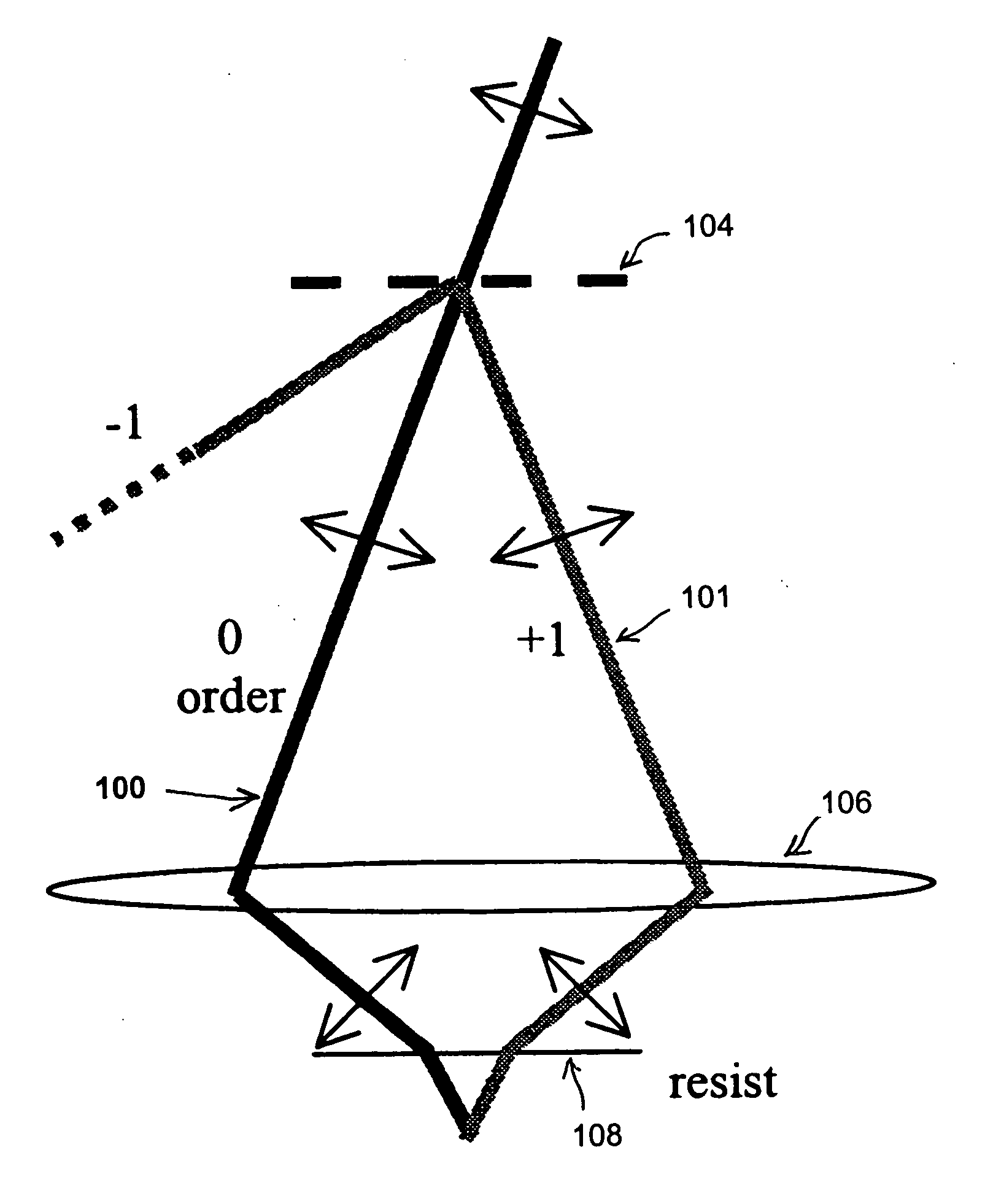
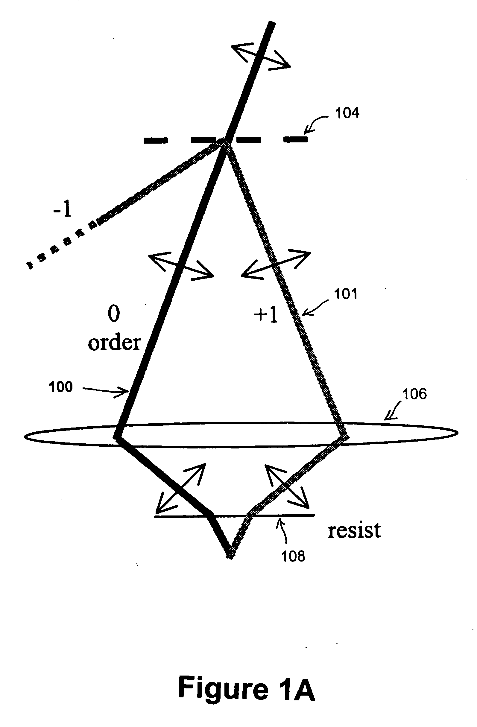
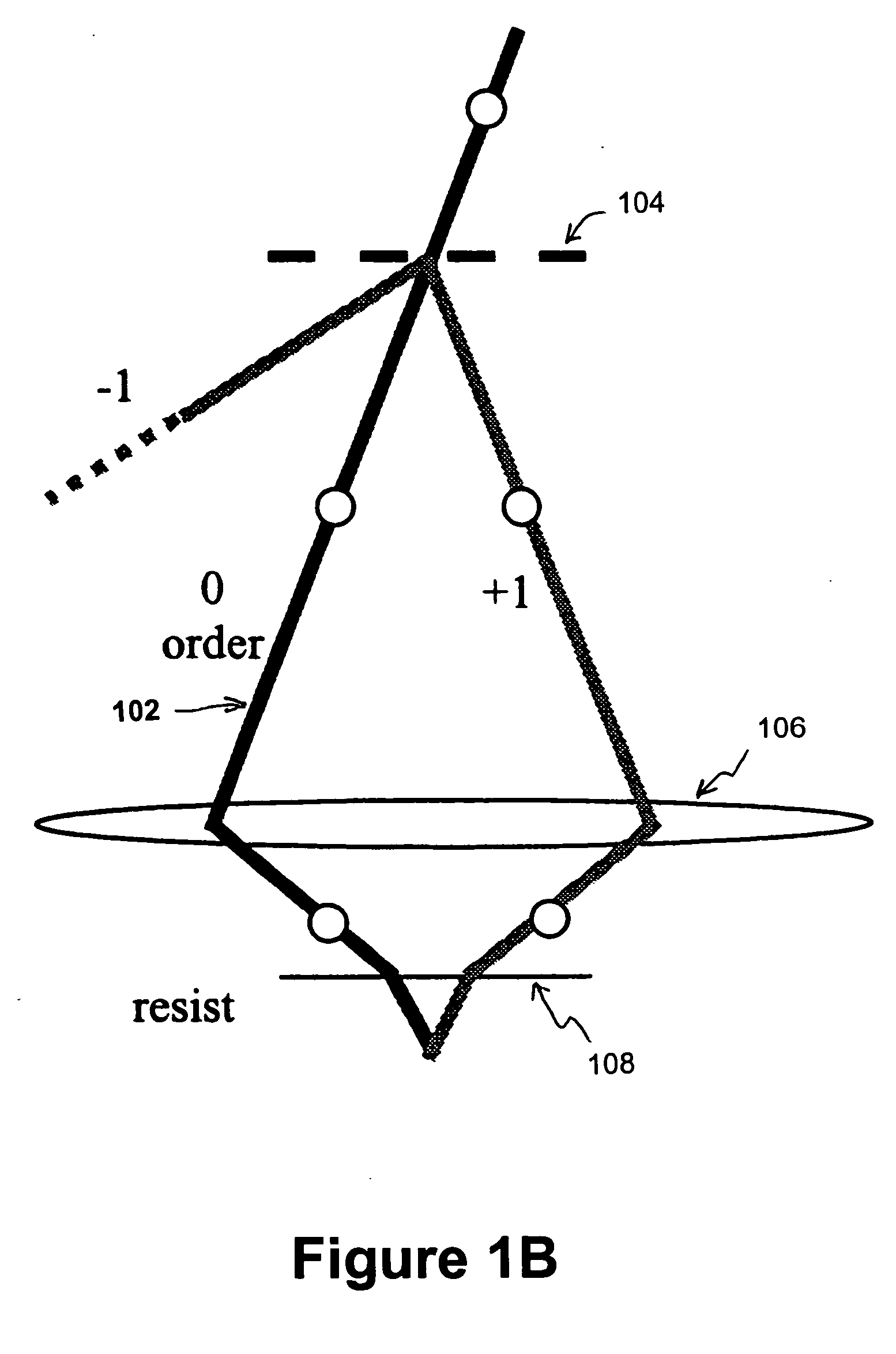
[0020] Embodiments of the present invention provide, among other things, an improved polarization system and method useful in high-precision lithography. Exemplary embodiments will now be described in detail with reference to the drawings, starting with FIGS. 1A and 1B.
[0021] In a high-precision lithography system, an image is projected onto a resist material. The amount of interference generating this image determines the level of contrast. In particular, a higher percentage of interfering light will produce greater contrast. Light interferes only when it is coherent and the electric fields are parallel. Therefore, components whose vibration energies are parallel provide greater contrast. The orientation of the polarization vector in lithography systems therefore determines contrast and affects the performance of the system.
[0022]FIGS. 1A and 1B illustrate the effect of these factors on imaging in a lithography system. FIG. 1A shows an optical path arrangement that produces a rel...
PUM
 Abstract
Description
Claims
Application Information