Multi-wavelength semiconductor laser device

a laser device and multi-wavelength technology, applied in semiconductor lasers, laser details, laser optical resonator construction, etc., can solve the problems of increased operation current of ld requiring a low output, unfavorable phenomena, gain saturation and catastrophic optical damage (cod), etc., to achieve sufficient resonant length, reduce operation current, and increase the degree of device integration

Inactive Publication Date: 2006-05-04
SAMSUNG ELECTRONICS CO LTD
View PDF8 Cites 3 Cited by
  • Summary
  • Abstract
  • Description
  • Claims
  • Application Information

AI Technical Summary

Benefits of technology

[0018] The present invention provides an improved multi-wavelength semiconductor laser device comprising a high-output LD and a low-output LD integrated on one substrate wherein the high-output LD has a sufficient resonant length, the low-output LD has a reduced operation

Problems solved by technology

Accordingly, there is a problem in that an increase in the operation current of the LD requiring a low output is inevitable.
Accordingly, the first and second LDs A and B have the same resonant length L. At this time, unfavorable phenomena, such as gain saturation and catastrophic optical damage (COD), may take place in the high-output LD due to increased current density.
The unnecessarily

Method used


Image

  • Multi-wavelength semiconductor laser device
  • Multi-wavelength semiconductor laser device
  • Multi-wavelength semiconductor laser device

Examples


Embodiment Construction

[0026] Detailed description will be made of embodiments of the present invention with reference to the accompanying drawings. However, various modifications to the embodiments of the present invention may easily be made, and the scope of the present invention is not limited by the following embodiments. These embodiments are provided to those skilled in the art for a better understanding of the present invention. In the drawings, the shape and size of elements may be exaggerated for the purpose of clarity, and the same elements are denoted by the same reference numerals even though they are depicted in different drawings.

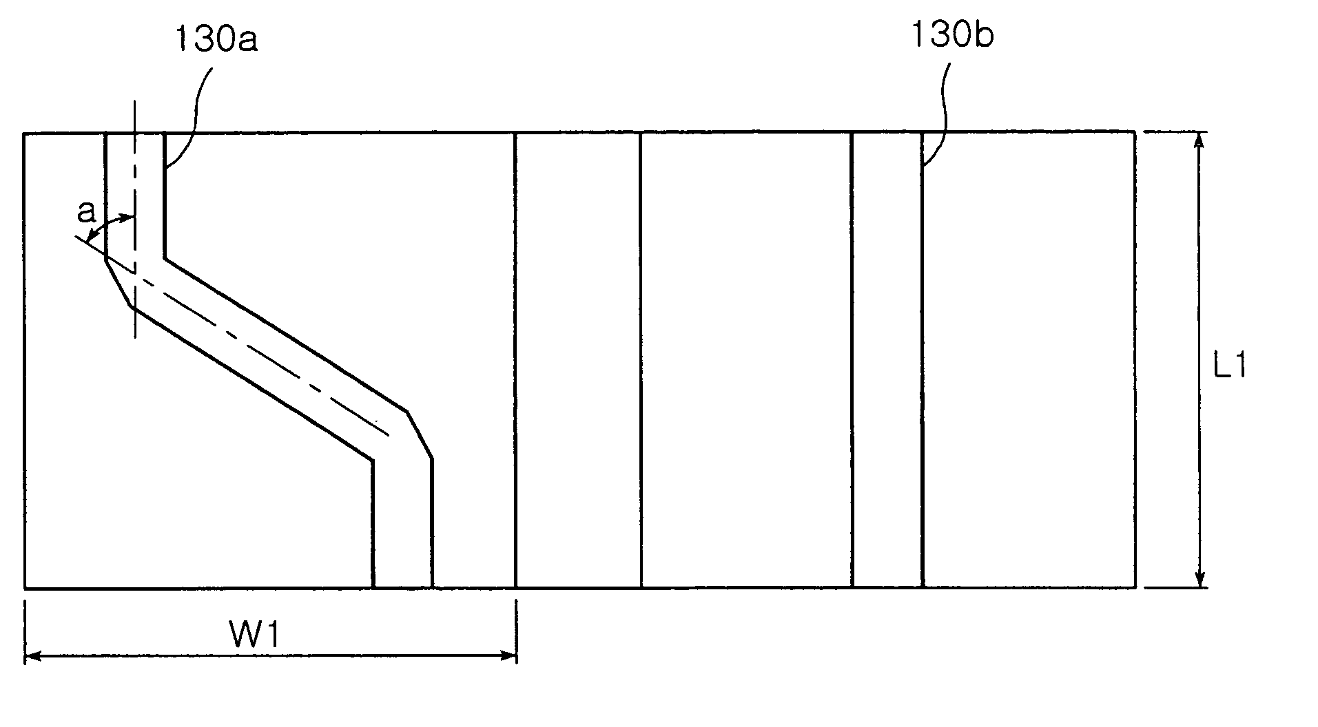
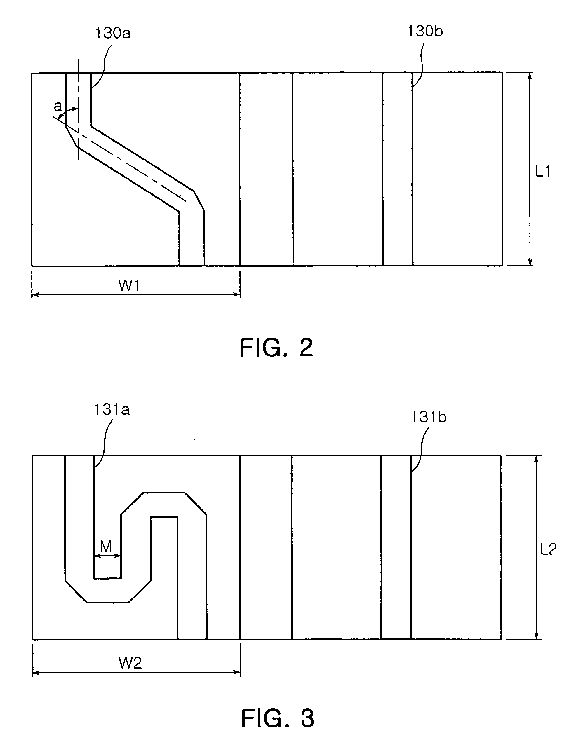
[0027]FIG. 2 is a plan view of a two-wavelength semiconductor laser device according one embodiment of the present invention. Referring to FIG. 2, the left and right regions correspond to a high-output LD and a low-output LD, respectively. A ridge structure 130a bent at two bending positions is formed in the high-output LD, and a ridge structure 130b having no bent...


PUM


Abstract

A semiconductor laser device comprises: a substrate having a top surface divided into a first region and a second region; a high-output LD including a first conductivity-type clad layer, an active layer, and a second conductivity-type clad layer including an upper portion having a first ridge structure, sequentially formed on the first region of the substrate; and a low-output LD including a first conductivity-type clad layer, an active layer, and a second conductivity-type clad layer including an upper portion having a second ridge structure, sequentially formed on the second region of the substrate, wherein the first and second ridge structures are formed in such a manner that they are extended to both ends opposed to each other, the first ridge structure is bent at two or more bending positions, and the second ridge structure is rectilinear.

Description

RELATED APPLICATIONS [0001] The present application is based on, and claims priority from, Korean Application Number 2004-87199, filed Oct. 29, 2004, the disclosure of which is incorporated by reference herein in its entirety. BACKGROUND OF THE INVENTION [0002] 1. Field of the Invention [0003] The present invention relates to a semiconductor laser device, and more particularly to a multi-wavelength semiconductor laser device capable of reducing operation current of a low-output semiconductor laser diode while providing a sufficient resonant length to a high-output semiconductor laser diode. [0004] 2. Description of the Related Art [0005] A general semiconductor laser device comprises p-type and n-type clad layers for current injection, and an active layer disposed between the clad layers in which induced emission of photons substantially occurs. Since an upper clad layer of the general semiconductor laser device is formed into a ridge structure, current injection efficiency is impro...

Claims


Application Information

Patent Timeline
IPC IPC(8): H01S5/00
CPCH01S3/08086H01S3/0809H01S5/4025H01S5/10H01S5/30
Inventor MOON, KI WONOH, HYE RANPARK, JONG IKKIM, YU SEUNG
Owner SAMSUNG ELECTRONICS CO LTD
Why Eureka
Try Eureka