Method and apparatus for fabricating and connecting a semiconductor power switching device

Active Publication Date: 2006-05-11
WOODWARD GOVERNOR CO
View PDF3 Cites 4 Cited by
  • Summary
  • Abstract
  • Description
  • Claims
  • Application Information

AI Technical Summary

Benefits of technology

[0008] Still another embodiment of the present invention relates to the manner in which the device can be easily mounted on a printed circuit board by providing conductive lands on the printed circuit board that are coextensive with metallized electrodes on the device and which can be placed on the printed circuit board and soldered in place.
[0009] Still another embodiment relates to a unique lead frame which can be soldered to another electrode metallization on the opposite side of the chip and the printed circuit board in a m

Problems solved by technology

Thermal performance of current art solid state ignition exciters has been limited due to available thyristor switching technology.
However, performance of both suffer from leakage current related limitations of the switching devices.
At elevated temperatures, leakage current within the switching device results in increased power dissipation.
This condition precipitates additional leakage current, resulting in a

Method used


Image

  • Method and apparatus for fabricating and connecting a semiconductor power switching device
  • Method and apparatus for fabricating and connecting a semiconductor power switching device
  • Method and apparatus for fabricating and connecting a semiconductor power switching device

Examples


Example

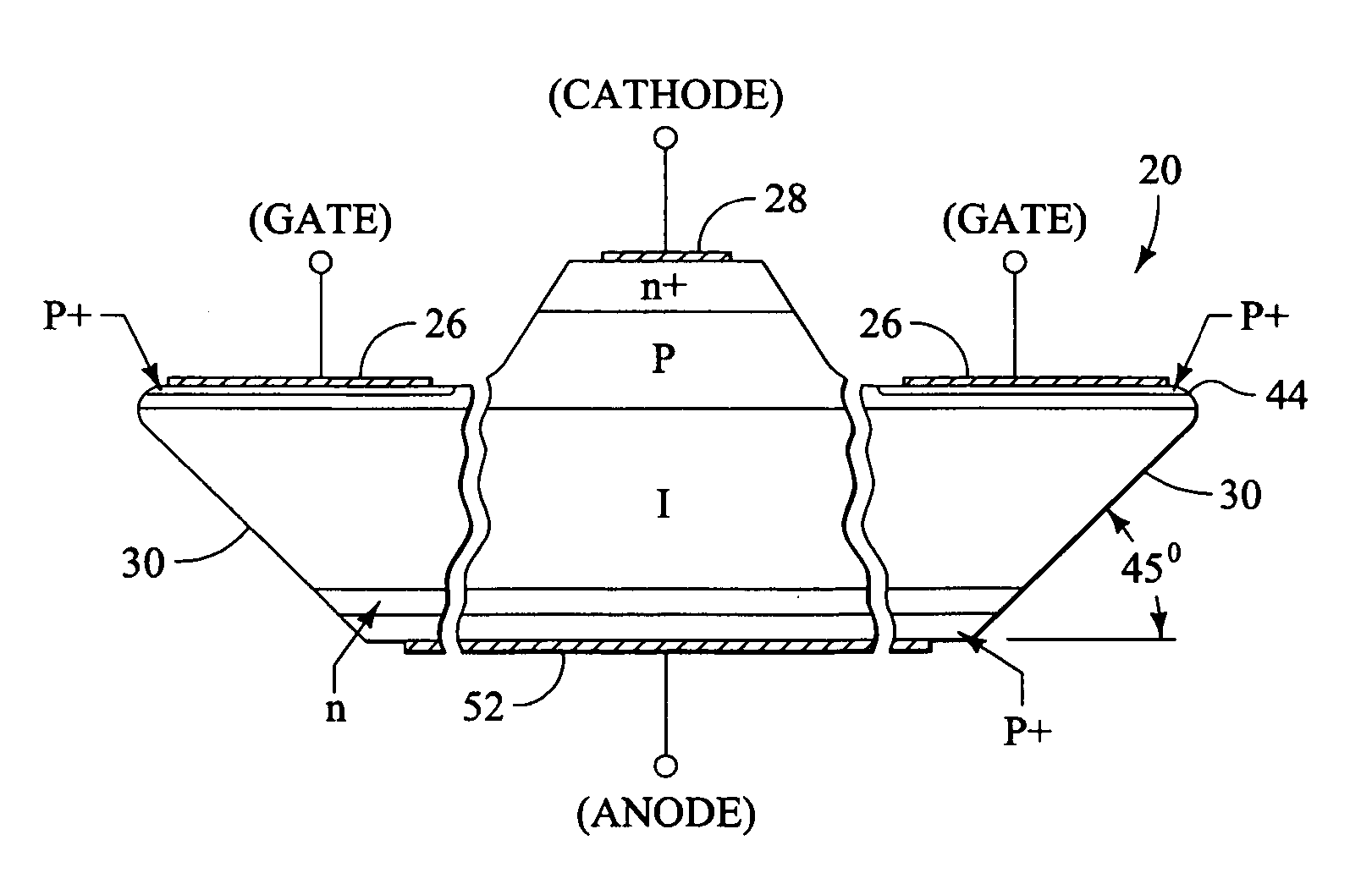
[0028] While the present invention relates to a semiconductor pulse switching device that is particularly useful in implementing exciter circuitry for turbine engine ignition systems and particularly aircraft engine ignition exciter circuits, the fabrication processes and techniques that are described herein are applicable to fabricating and connecting other semiconductor devices having other applications. However, the processes and apparatus that are disclosed herein are particularly configured for use in high power circuitry where large currents may flow for short periods of time. Because high load transitory conditions may be commonplace for such devices, the fabrication and connecting processes and apparatus described herein may be useful across a wide variety of applications where high current flow may occur.

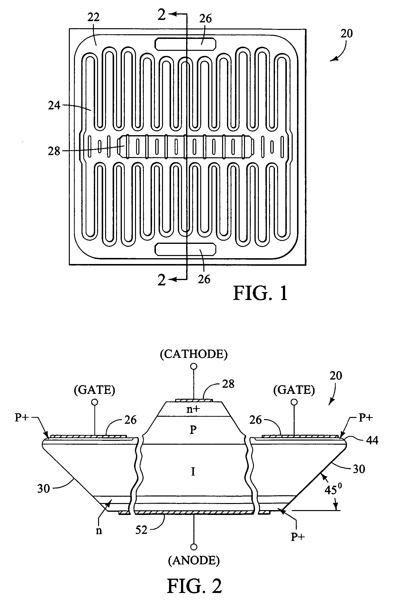
[0029] Referring to FIG. 1, an exemplary PSD switching device is illustrated generally at 20. The highly interdigitated gate-cathode structure of this device allows direct...


PUM

PropertyMeasurementUnit
Angleaaaaaaaaaa
Lengthaaaaaaaaaa
Angleaaaaaaaaaa

Abstract

Fabrication processes for manufacturing and connecting a semiconductor switching device are disclosed, including an embodiment for dicing a wafer into individual circuit die by sawing the interface between adjacent die with a saw blade that has an angled configuration across its width, preferably in a generally V-shape so that the adjacent die are severed from one another while simultaneously providing a beveled surface on the sides of each separated die. Another embodiment relates to the manner in which damage to a beveled side surface of the individual die can be smoothed by a chemical etching process. Another embodiment relates to the manner in which the device can be easily mounted on a printed circuit board by providing conductive lands on the printed circuit board that are coextensive with metallized electrodes on the device and which can be placed on the printed circuit board and soldered in place and a unique lead frame which can be soldered to another electrode metallization on the opposite side of the chip and the printed circuit board in a manner which substantially reduces if not eliminates harmful thermal stress and which assures secure bonding notwithstanding elevation differences between the electrode metallization and the printed circuit board the lead frame is attached to. Another embodiment relates to an output connector for interconnecting an exciter circuit product with a spark producing device wherein the output connector utilizes a configuration that includes a sealing structure that is reliable and easily installed.

Description

CROSS REFERENCE TO RELATED APPLICATIONS [0001] A Solid State Turbine Engine Ignition Exciter Having Elevated Temperature Operational Capability, filed Jun. 15, 2004, Ser. No. 10 / 868,621, by Theodore S. Wilmot, John C. Driscoll and Richard S. Brzostek. BACKGROUND OF THE INVENTION [0002] The present invention generally relates to semiconductor fabrication and connection methods and apparatus, and more particularly to fabrication and connection methods and apparatus high voltage semiconductor power switching devices that are useful in ignition exciters for turbine engine applications. [0003] Modern turbine engine ignition exciters, especially those used in small gas turbine applications, have evolved considerably in recent years; migrating from spark gap (plasma) switching devices and simple relaxation type oscillator charge pumps to more reliable and predictable solid state switching devices with digitally controlled DC-DC converter charge pumps. Thermal performance of current art sol...

Claims


Application Information

Patent Timeline
IPC IPC(8): H01L23/495
CPCB28D1/121B28D5/022H01L21/78H01L2924/10158H01L2924/0002H01L2924/00
Inventor WILMOT, THEODORE S.DRISCOLL, JOHN C.BRYAN, EUGENE N.
Owner WOODWARD GOVERNOR CO
Why Eureka
Try Eureka