

Optical element mold and the process for making such
a technology of optical elements and molds, applied in the field of molds for making optical elements, can solve the problems that the dlc film on the mold cannot be expected to provide a satisfactory performance, and the results are not ideal, so as to achieve better fracture toughness, longer operating life, and more wear resistance
- Summary
- Abstract
- Description
- Claims
- Application Information
AI Technical Summary
Benefits of technology
Problems solved by technology
Method used
Image

Examples
Embodiment Construction
[0015] Reference will now be made to the drawings to describe the preferred embodiments of the present mold and the manufacture thereof, in detail.
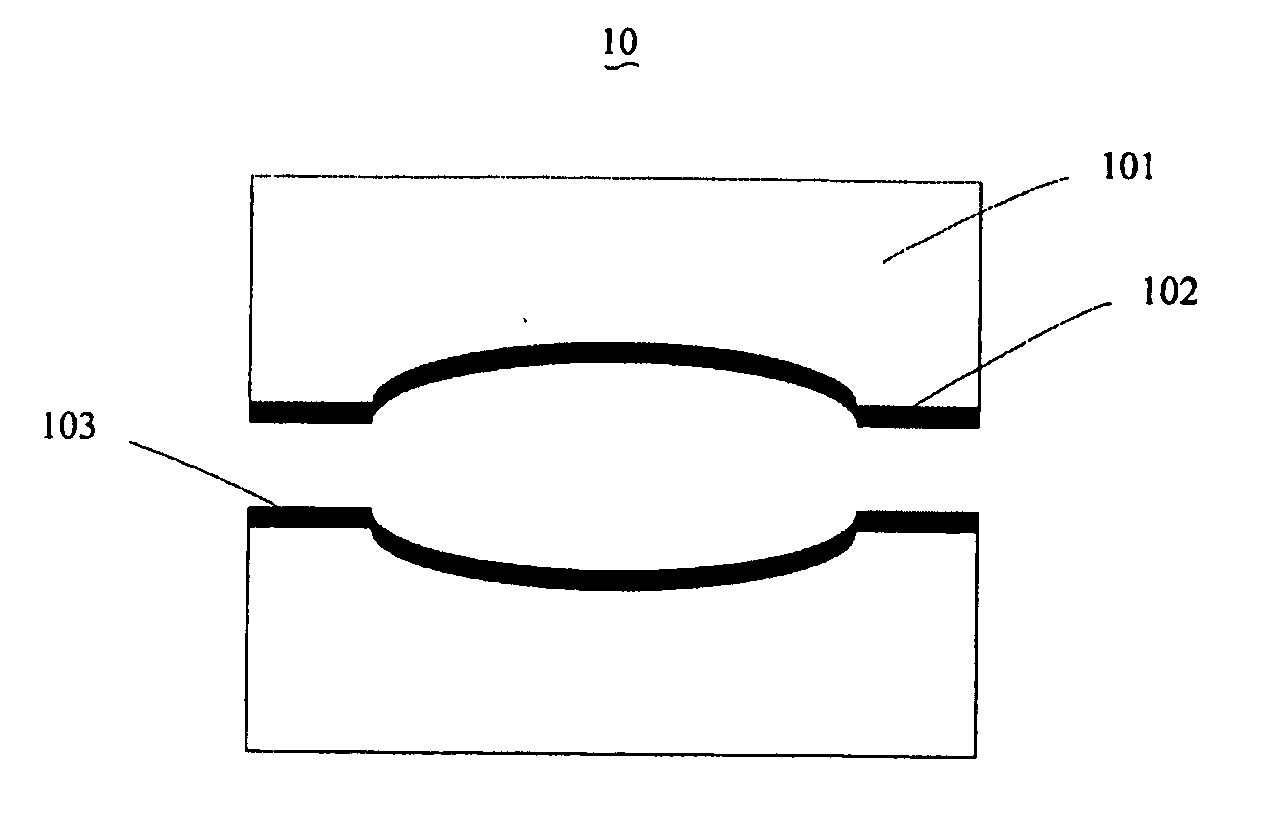
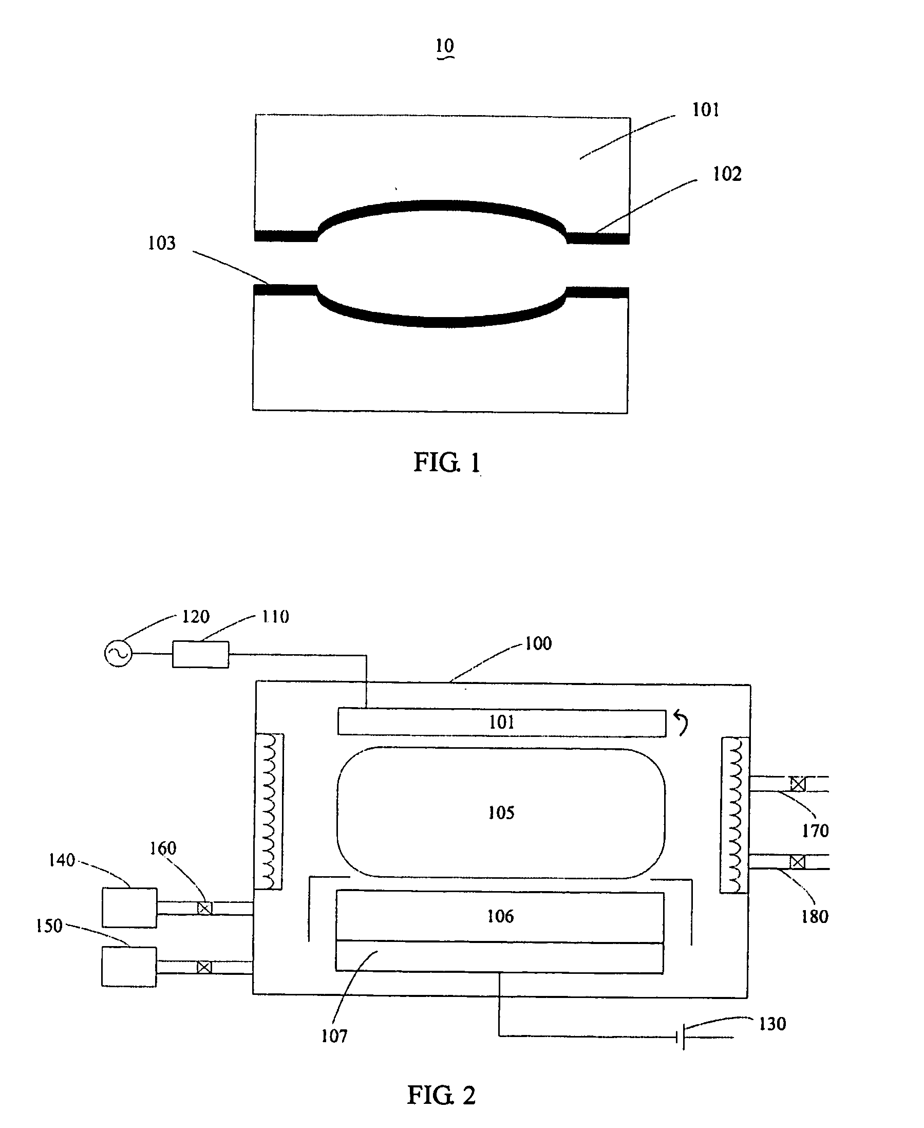
[0016] Referring now to the drawings, and more particularly to FIG. 1, there is shown an optical element mold 10, according to one embodiment. The optical element mold 10 has a mold base 101 and a coating layer 103 formed on a surface layer 102 of the mold base 101. The surface layer 102 is advantageously made of a tungsten carbide (WC) ceramic (e.g., WC or a WC-based composite). However, it is to be understood that any other carbide ceramic or other ceramic material that would promote the formation of a coating layer 103 having the desired properties would be within the scope of the present invention.
[0017] The coating layer 103 is substantially comprised of nano-scale crystalline particles enclosed and bordered by nano-scale crystalline boundaries (i.e., coating layer 103 being a polycrystalline material with both nano-scale grains an...
PUM
| Property | Measurement | Unit |
|---|---|---|
| thickness | aaaaa | aaaaa |
| compressive stress | aaaaa | aaaaa |
| compressive stress | aaaaa | aaaaa |
Abstract
Description
Claims
Application Information