
Internal voltage generator for semiconductor memory device

a technology of semiconductor memory devices and voltage generators, which is applied in the direction of pulse generators, pulse techniques, instruments, etc., can solve the problems of increasing the voltage level of the internal voltage vpp undesirably higher than the target level, increasing the variation width of the level of the internal voltage vpp, and increasing the noise of the internal operation. , to achieve the effect of reducing the variation width in the level

Inactive Publication Date: 2006-05-11
SK HYNIX INC
View PDF0 Cites 15 Cited by
  • Summary
  • Abstract
  • Description
  • Claims
  • Application Information

AI Technical Summary

Benefits of technology

[0012] Accordingly, an internal voltage generator is disclosed which is capable of reducing the variation width in the level of an internal voltage VPP by performing charge pumping only a predetermined number of times even when an oscillator driving signal is at a logic HIGH level, and then stopping the charge pumping operation.

Problems solved by technology

As semiconductor memory devices become faster and lower in power usage, internal operation becomes very sensitive to noise.
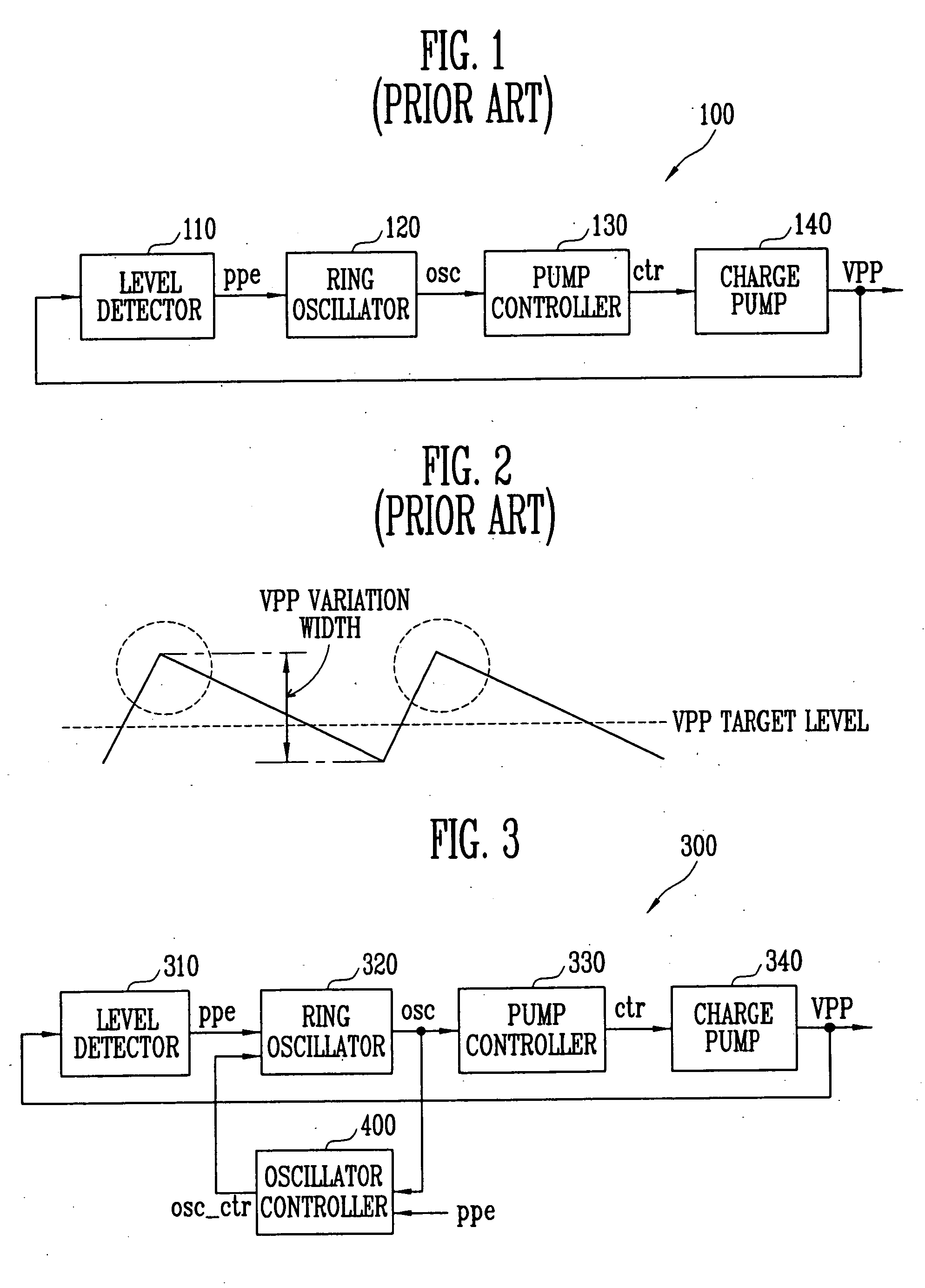
In this case, there is a problem in that the voltage level of the internal voltage VPP undesirably increases higher than the target level because the charge pumping operation continues.
Accordingly, there is a problem in that the variation width in the level of the internal voltage VPP is greater.

Method used


Image

  • Internal voltage generator for semiconductor memory device
  • Internal voltage generator for semiconductor memory device
  • Internal voltage generator for semiconductor memory device

Examples


Embodiment Construction

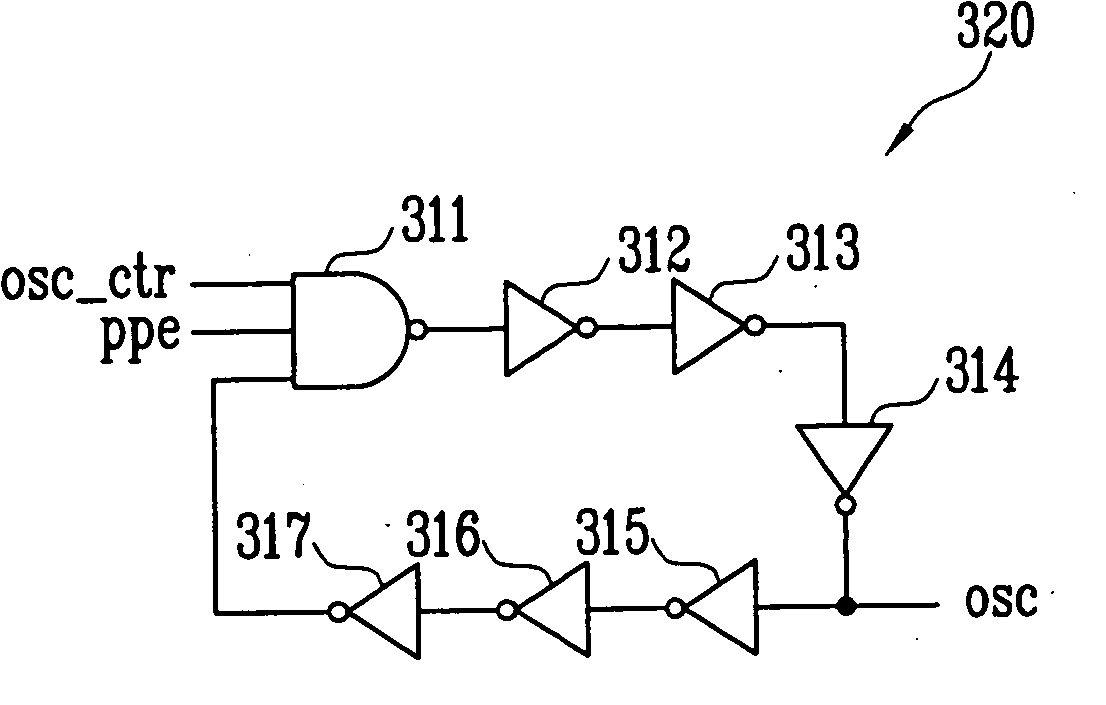
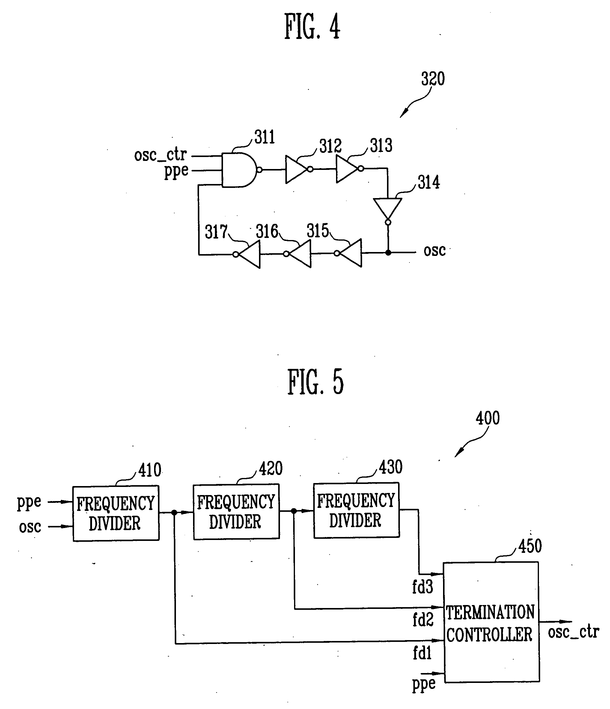
[0024]FIG. 3 is a block diagram illustrating the configuration of a disclosed internal voltage generator. The internal voltage generator 300 includes a level detector 310, a ring oscillator 320, a pump controller 330, a charge pump 340 and an oscillator controller 400.

[0025] The level detector 310 detects the level of an internal voltage VPP to generate an oscillator driving signal ppe. The ring oscillator 320 generates an oscillation signal osc using the oscillator driving signal ppe. The oscillator controller 400 generates an oscillation control signal osc_ctr for stopping an oscillation operation at a predetermined time point using the oscillation signal osc, even when the oscillator driving signal ppe is at a HIGH level. The oscillation control signal osc_ctr generated thus is again input to the ring oscillator 320. The ring oscillator 350 does not generate the oscillation signal osc at a predetermined time point in a period where the oscillator driving signal ppe is at a HIGH ...


PUM


Abstract

An internal voltage generator capable of reducing the variation width in the level of an internal voltage VPP, by performing charge pumping only a predetermined number of times in a period where an oscillator driving signal is at a logic HIGH level, and then stopping the charge pumping operation. The oscillator controller generates an oscillation control signal for stopping an oscillation operation of a ring oscillator by using an output signal of a level detector and an output signal of the ring oscillator. The ring oscillator does not generate an oscillation signal at a predetermined time point where an output signal of the level detector is at a HIGH level in response to the oscillation control signal. The charge pump circuit generates an internal voltage by performing a charge pumping operation only predetermined times in response to the oscillation signal, and then stopping the charge pumping operation.

Description

BACKGROUND [0001] 1. Technical Field [0002] An internal voltage generator for generating a high voltage VPP or a substrate voltage in a semiconductor memory device is shown and described. [0003] 2. Description of the Related Art [0004] As semiconductor memory devices become faster and lower in power usage, internal operation becomes very sensitive to noise. Semiconductor memory, particularly DRAM devices, usually include an internal voltage generator for generating an internal voltage of a predetermined level for the internal operation in addition to an external input voltage. An internal voltage generator can generate a voltage higher than an external high voltage, i.e., a high voltage VPP, or a voltage lower than an external low voltage (usually, ground voltage), i.e., a back bias voltage or a substrate voltage. An internal voltage generator generates an internal voltage of a predetermined level by employing a charge pumping mode. [0005]FIG. 1 is a block diagram illustrating the c...

Claims


Application Information

Patent Timeline
Patent Type & Authority Applications(United States)
IPC IPC(8): H03K3/03
CPCH02M3/073H02M2001/0041H02M1/0041G11C5/14
Inventor IM, JAE HYUKLEE, JAE JIN
Owner SK HYNIX INC
Learn More