Level detector, communication apparatus, and tuner

a level detector and communication apparatus technology, applied in the field of level detectors, can solve the problems of not being able to distinguish the waveform from another low-strength waveform, unable to remove the high-strength component that rarely appears, and unable to achieve waveforms in which the strength fluctuates extremely sharply, so as to reduce the variation generated, reduce the variation in the width of the pulse output, and reduce the variation

Inactive Publication Date: 2008-08-07
SHARP KK
View PDF0 Cites 10 Cited by
  • Summary
  • Abstract
  • Description
  • Claims
  • Application Information

AI Technical Summary

Benefits of technology

[0021]In the level detector of the present invention, the pulse width extending circuit preferably further comprises a second diode having substantially the same circuit characteristics as the first diode; a second resistor having substantially the same circuit characteristics as the first resister; and a pulse width extending comparator. The pulse width extending comparator comprises,a first input terminal connected to the cathode of the first diode, and a second input terminal connected to both of the second diode and the second resistor. The pulse width extending comparator outputs to the integrating circuit a pulse corresponding to the length of a time period during which the voltage at the first input terminal is higher than the voltage at the second input terminal. In this case, the second diode and resistor are preferably connected to the second input terminal so as to reduce variation generated in the width of the pulse to be output from the pulse width extending comparator, due to at least one of the circuit characteristics and temperature variations of the first diode and resistor. The forward voltage of a diode may widely vary due to variations in the temperatures of the diode itself and the corresponding resistor, and the manufacturing variations in them. This may brings about variation in the time period for the discharge of the capacitor, and thus variation in the width of a pulse output from the pulse width extending circuit. In this feature of the present invention, however, the second diode and resistor having the same circuit characteristics as the respective first diode and resistor connected to the first terminal, are connected to the second terminal so as to reduce variation in the width of the pulse output from the pulse width extending circuit. This reduces variation generated in the pulse output from the pulse width extending circuit due to the circuit characteristics and the temperature variation.
[0022]A level detector of the present invention preferably comprises a signal input; a first comparing circuit that generates a signal comprising a plurality of temporally successive pulses each having its width corresponding to the length of a time period during which the strength of an input signal from the input is higher than a first reference value; a second comparing circuit that generates a signal comprising a plurality of temporally successive pulses each having its width corresponding to the length of a time period during which the strength of the input signal from the input is lower than a second reference value lower than the first reference value; an OR circuit that generates a signal having its strength corresponding to the logical sum of the signal generated by the first comparing circuit and the signal generated by the second comparing circuit; a pulse width extending circuit that generates a signal in which each pulse contained in the signal generated by the OR circuit has been temporally extended; and an integrating circuit that outputs a signal having its strength corresponding to an integration value obtained by temporally integrating the strength of the signal generated by the pulse width extending circuit. In this feature of the present invention, the OR circuit outputs a pulse in either of the case in which the strength of the input signal is higher than the first reference value; and the case in which the strength of the input signal is lower than the second reference value lower than the first reference value. Therefore, when the DC voltage of the input signal varies, the frequency of appearance of pulses increases in one of the first and second comparing circuits while the frequency of appearance of pulses decreases in the other of the first and second comparing circuits. Thus, even when the DC voltage varies, variation in the frequency of appearance of pulses is suppressed. This suppresses detection error in the signal strength.
[0023]A level detector of the present invention preferably comprises first to n-th signal inputs corresponding to n input signals, where n represents a natural number more than one; first to n-th comparing circuits each of which generates a signal comprising a plurality of temporally successive pulses each having its width corresponding to the length of a time period during which the strength of an input signal from the corresponding one of the first to n-th inputs is higher than a first reference value; an OR circuit that generates a signal having its strength corresponding to the logical sum of the signals generated by the first to n-th comparing circuits; a pulse width extending circuit that generates a signal in which each pulse contained in the signal generated by the OR circuit has been temporally extended; and an integrating circuit that outputs a signal having its strength corresponding to an integration value obtained by temporally integrating the strength of the signal generated by the pulse width extending circuit. This feature of the present invention is effective to a case in which the DC voltage increases in one of the input signals while the DC voltage decreases in another input signal. For example, when an DC offset voltage is generated between the components of a differential signal, the DC voltage of one component of the differential signal increases while the DC voltage of the other component of the differential signal decreases. In the above feature of the present invention, however, of the first to n-th comparing circuits, the frequency of appearance of pulses increases in the comparing circuit to which the signal whose DC voltage has increased while the frequency of appearance of pulses decreases in the comparing circuit to which the signal whose DC voltage has decreased. This eliminates the influence of the offset voltage on the frequency of appearance of pulses.

Problems solved by technology

In a signal demodulated by the OFDM method, however, because the signal band has been restricted, there is obtained no waveform in which the strength varies extremely sharply.
Therefore, even if such a high-strength component is intended to be removed, the waveform can not be distinguished from another low-strength waveform.
Thus, the charge / discharge circuit 903 can not remove the high-strength component that rarely appears.
This may make it impossible to obtain an average strength.
Consequently, the level detector 900 is unsuitable for a receiving circuit of a mobile communication device according to, for example, the OFDM method.
Therefore, when the average strength of an OFDM signal input to the level detector 900 is low and the S / N ratio to noise generated in the receiving circuit is insufficient, the influence of the noise appearing in the integration result may increase.
This makes it hard to accurately indicate the average strength of the received signal.

Method used


Image

  • Level detector, communication apparatus, and tuner
  • Level detector, communication apparatus, and tuner
  • Level detector, communication apparatus, and tuner

Examples


first embodiment

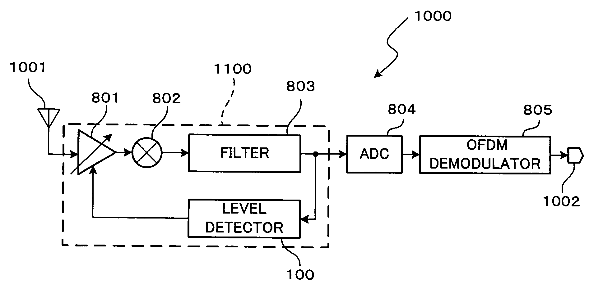
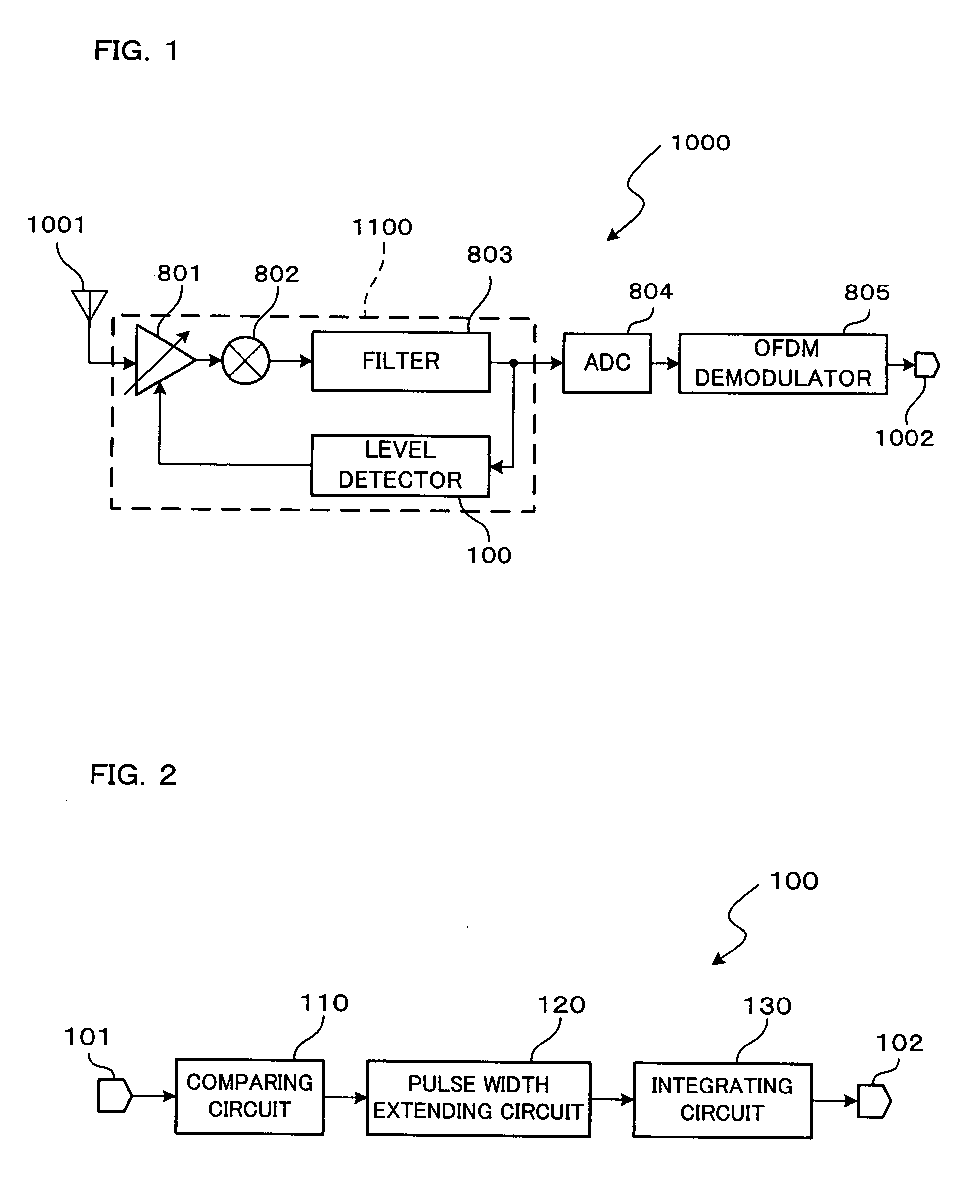
[0037]The receiver 1000 includes an antenna unit 1001, a tuner unit 1100, an analog-to-digital converter (ADC) circuit 804, and an OFDM demodulator 805. An OFDM-modulated signal is input to the tuner unit 1100 through the antenna unit 1001. The tuner unit 1100 applies a channel selecting process to the OFDM-modulated signal. The channel-selecting-processed signal is input to the ADC circuit 804. The ADC circuit 804 converts the channel-selecting-processed signal from an analogue signal into a digital signal. The converted digital signal is input to the OFDM demodulator 805. The OFDM demodulator 805 demodulates the digital signal into a data string signal. The demodulated data string signal is output through an output terminal 1002 to the exterior of the receiver 1000.

[0038]The tuner unit 1100 includes therein a variable gain amplifier (VGA) 801, a mixer circuit 802, a filter circuit 803, and a level detector 100. The received signal sent from the antenna unit 1001 is amplified by th...

second embodiment

[0073]Next, a second embodiment of the present invention will be described with reference to FIG. 6. FIG. 6 is a circuit diagram showing a construction of a pulse width extending circuit 320 according to the second embodiment. In the second embodiment, the pulse width extending circuit 120 of the first embodiment is replaced by the pulse width extending circuit 320. The description of the parts other than the parts different from the first embodiment will be arbitrarily omitted below. The same components as in the first embodiment are denoted by the same references as in the first embodiment, respectively.

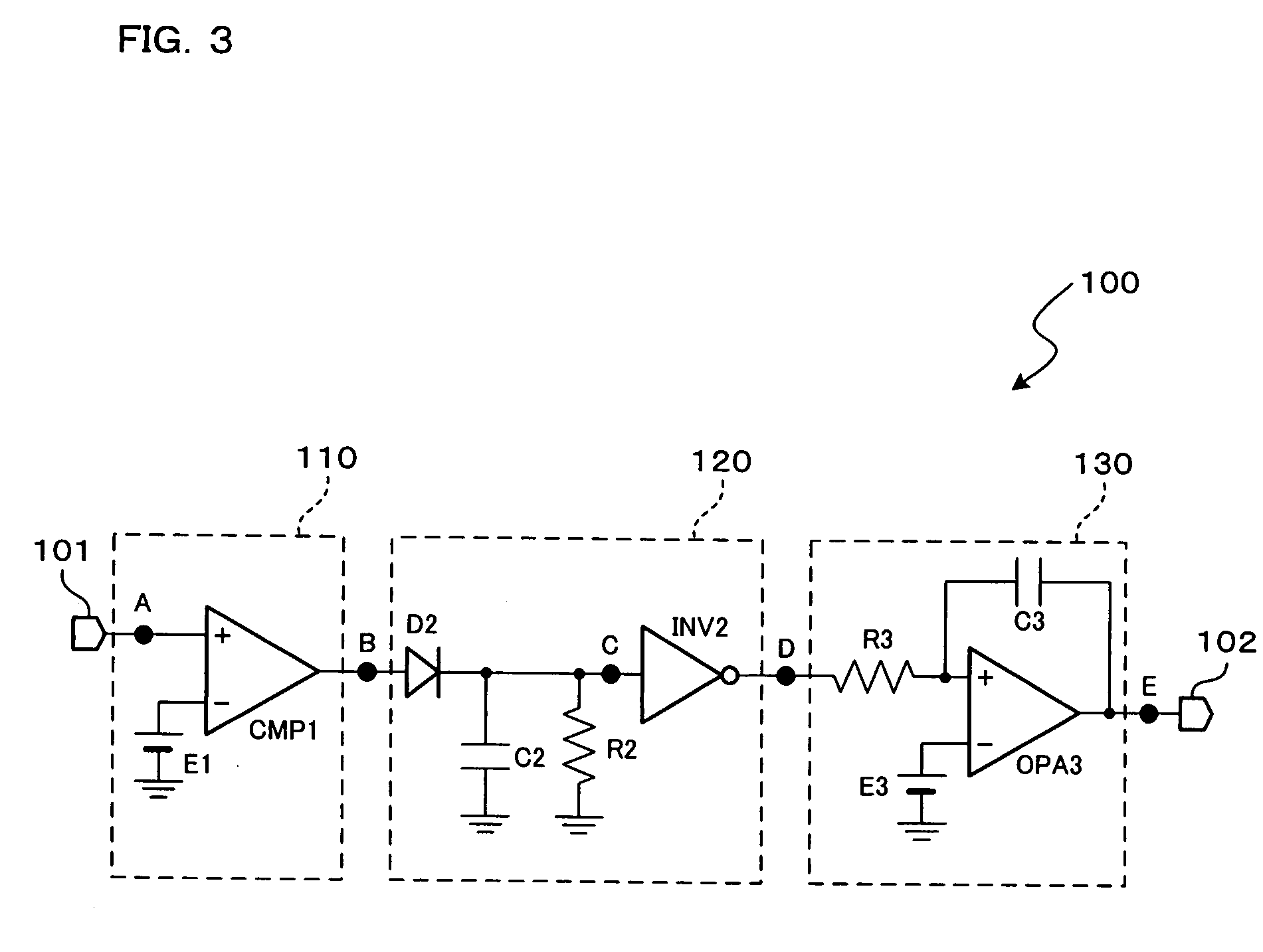
[0074]The pulse width extending circuit 320 includes therein a diode D2, a capacitor C2, a resistor R2, and a comparator CMP2. The anode of the diode D2 is connected to the output terminal of the comparing circuit 110 through an input terminal 321. Either of one ends of the capacitor C2 and the resistor R2 is connected to the cathode of the diode D2. Either of the other ends of the...

third embodiment

[0082]Next, a third embodiment of the present invention will be described with reference to FIG. 7. FIG. 7 is a circuit diagram showing a construction of a comparing circuit 410 according to the third embodiment. In the third embodiment, the comparing circuit 110 of the first embodiment is replaced by the comparing circuit 410. The description of the parts other than the parts different from the first embodiment will be arbitrarily omitted below. The same components as in the first embodiment are denoted by the same references as in the first embodiment, respectively.

[0083]An OFDM signal is input to the comparing circuit 410 from the filter circuit 803 through an input terminal 411. The comparing circuit 410 includes therein comparators CMP1 and CMP11; DC power supplies E1 and E11; and an OR circuit OR1. The non-inverting input of the comparator CMP1 and the inverting input of the comparator CMP11 are connected to the input terminal 411. The inverting input of the comparator CMP1 is...


PUM


Abstract

A level detector includes a comparing circuit and an integrating circuit. The comparing circuit generates pulses each having its width corresponding to the length of a time period during which the strength of an input signal is higher than a reference value. Alternatively, the comparing circuit may generate pulses each having its width corresponding to the length of a time period during which the strength of the input signal is lower than the reference value. The comparing circuit successively outputs the pulses. The integrating circuit outputs a signal having its strength corresponding to an integration value obtained by temporally integrating the signal from the comparing circuit.

Description

BACKGROUND OF THE INVENTION[0001]1. Field of the Invention[0002]The present invention relates to a level detector that outputs a signal to indicate the strength of an input signal, and also to a communication apparatus and a tuner including therein the detector.[0003]2. Description of Related Art[0004]In a receiving or transmitting circuit in a communication apparatus, the gain of an amplifier must be controlled in order that a received signal or a signal to be transmitted has the optimum level. For this purpose, a level detector is required to detect the average strength, that is, the average level, of the signal. For example, a level detector disclosed in Japanese Patent Unexamined Publication No. 2000-134163 outputs a received signal strength indication (RSSI) signal to indicate the strength of a received signal. The level detector of the publication has the following construction in order to reduce the detection error when the received signal varies on an envelope curve.[0005]FI...

Claims


Application Information

Patent Timeline
Patent Type & Authority Applications(United States)
IPC IPC(8): G06G7/18H04B7/00
CPCH04B17/318G06G7/18
Inventor KAWAMA, SHUICHI
Owner SHARP KK
Why Eureka
Try Eureka