Semiconductor light emitting device

Active Publication Date: 2006-05-11
MITSUBISHI ELECTRIC CORP
View PDF15 Cites 19 Cited by
  • Summary
  • Abstract
  • Description
  • Claims
  • Application Information

AI Technical Summary

Benefits of technology

[0023] An object of the present invention is to provide a semiconductor light emitting device having good FFP characteristic

Problems solved by technology

A problem is known in that light confinement in the active layer thus decreases relatively, causing characteristic degradation such as a significant increase in threshold value (cf.
As a result, it is known that the occurrence of cracks or dislocation become significant; Even when neither cracks or dislocation occurs, a great level of distortion occurs, which adversely affects the life of elements.
This case, however, inev

Method used


Image

  • Semiconductor light emitting device
  • Semiconductor light emitting device
  • Semiconductor light emitting device

Examples


first preferred embodiment

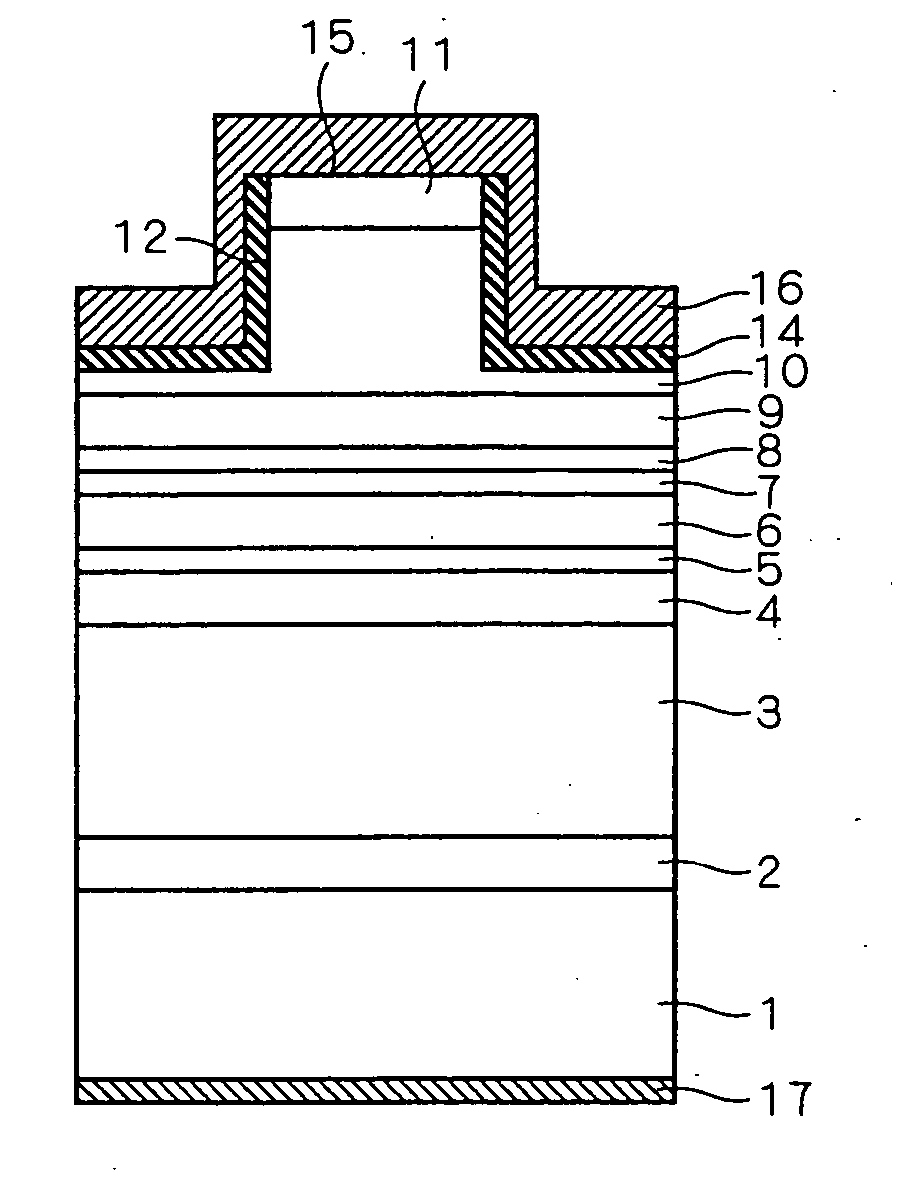
[0037]FIG. 1 is a sectional view illustrating the structure of a semiconductor light emitting device according to the present embodiment. This semiconductor light emitting device (nitride-based semiconductor laser) has a ridge structure and SCH structure.

[0038] An n-type GaN buffer layer 2 is formed on a Ga surface serving as a main surface of a GaN substrate 1 in order to reduce surface irregularities of the GaN substrate 1 to allow upper layers to be stacked thereon as flat as possible. An n-type AlGaN cladding layer (which may hereinafter be briefly referred to as an n-type cladding layer) 3 is formed on the n-type GaN buffer layer 2.

[0039] An n-type GaN optical guiding layer 4 and an undoped InGaN optical guiding layer 5 are stacked in this order on the n-type AlGaN cladding layer 3 to constitute an n-side optical guiding layer. On the InGaN optical guiding layer 5, an undoped active layer 6 of InxGa1-xN / InyGa1-yN multiple quantum well structure is formed, for example.

[0040] ...

second preferred embodiment

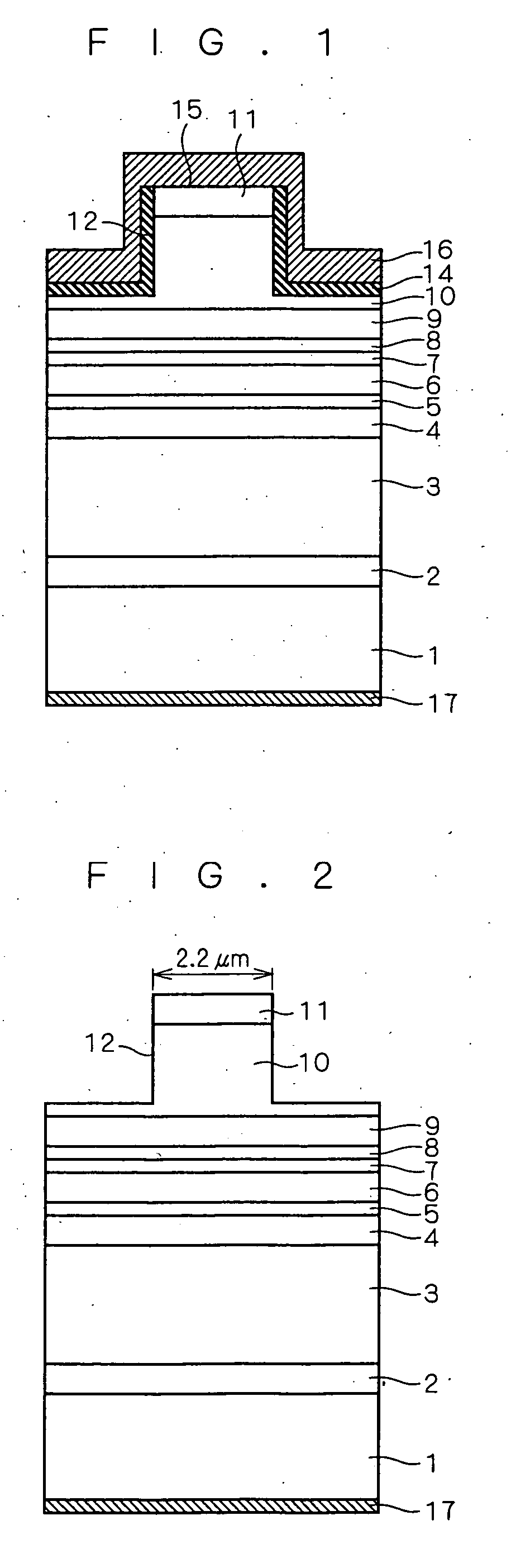
[0076] A semiconductor light emitting device according to the present embodiment is the semiconductor light emitting device according to the first preferred embodiment, but the n-type AlGaN cladding layer 3 has an Al composition ratio satisfying 0.01≦x<0.05 (see FIG. 1). The other structure is the same as that described in the first preferred embodiment, and repeated explanation is thus omitted here.

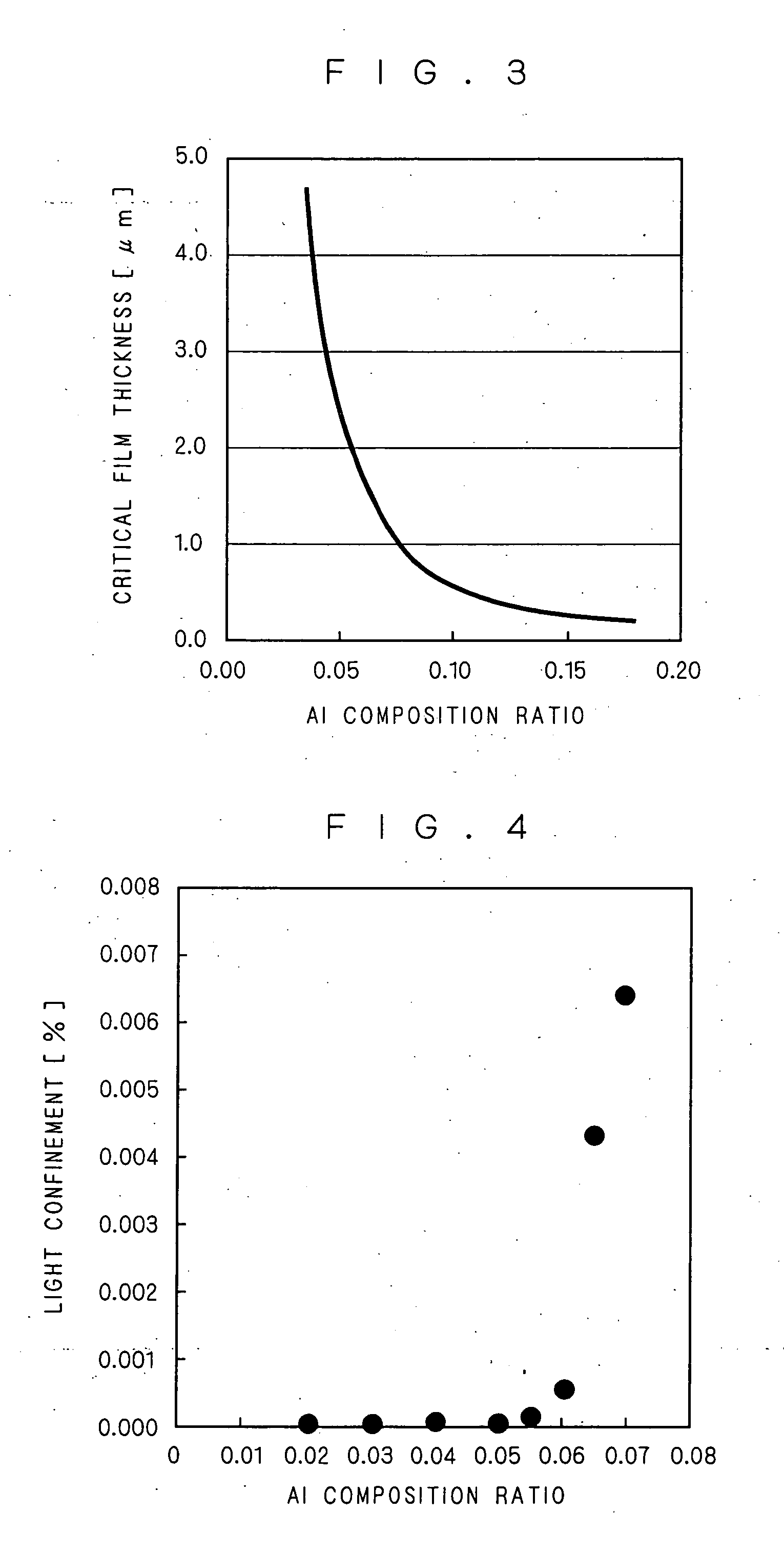
[0077] As shown in FIG. 3, the critical film thickness of the n-type cladding layer 3 greatly improves when the Al composition ratio becomes 0.05 or lower. Therefore, the n-type cladding layer 3 can be formed thicker without causing cracks or dislocation. As a result, as understood from FIGS. 4 and 5, the spreading of light into the GaN substrate 1 side can further be minimized.

[0078] Further, the refractive index increases by reducing the Al composition ratio x. Accordingly, NFP can spread out widely to reduce the full width at half maximum of FFP in the vertical direction.

[0079] In ...

third preferred embodiment

[0080]FIG. 7 is a sectional view illustrating a semiconductor light emitting device according to the present embodiment. In the present embodiment, an n-type cladding layer 13 (partial n-type AlGaN cladding layer) having an Al composition ratio higher than that of the n-type AlxGa1-xN cladding layer 3 (0.01≦x3 in the semiconductor light emitting device according to the first preferred embodiment. The other structure is the same as that of the first preferred embodiment. The same components are indicated by the same reference numerals, and repeated explanation thereof is thus omitted here.

[0081]FIG. 8 is a sectional view illustrating the distribution of light intensity in the vertical direction in the semiconductor light emitting device having the above-described structure. As shown in FIG. 8, the distribution of light intensity in the vertical direction is attenuated from the center of the active layer 6 toward the GaN substrate 1. The n-type cladding layer 13, having a refractive ...


PUM


Abstract

A semiconductor light emitting device including an active layer interposed between an n-type cladding layer and a p-type cladding layer employs an AlxGa1-xN (AlGaN) layer having an Al composition ratio x satisfying 0.01≦x<0.06 as the n-type cladding layer. As the Al composition ratio x decreases below 0.06, the AlGaN layer increases in refractive index. Thus, the near field pattern (NFP) in the vertical direction can spread out, and full width at half maximum of FFP in the vertical direction can be minimized. Further, since a lattice mismatch with a GaN substrate is reduced with decreasing Al composition ratio, the AlGaN layer can be formed thick without causing cracks or dislocation, and the spreading of light into the GaN substrate can be minimized.

Description

BACKGROUND OF THE INVENTION [0001] 1. Field of the Invention [0002] The present invention relates to a semiconductor light emitting device employing III-V nitride compound semiconductor. [0003] 2. Description of the Background Art [0004] In recent years, active research and development has been being conducted in semiconductor lasers employing III-V nitride compound semiconductor such as AlGaInN as semiconductor lasers capable of emitting light in an area ranging from the blue region to the ultraviolet region necessary for achieving higher density of optical disks, and such semiconductor lasers have already been put into practical use. [0005] Semiconductor lasers employing III-V nitride compound semiconductor which have been reported so far have a separate confinement heterostructure (SCH). [0006] More specifically, to effectively confine light in an active layer, an n-type AlGaN cladding layer made of a material having a relatively low refractive index is provided on the n-side, wh...

Claims


Application Information

Patent Timeline
IPC IPC(8): H01S5/00H01S5/343
CPCB82Y20/00H01S5/021H01S5/0213H01S5/2004H01S5/2009H01S5/22H01S5/3211H01S5/3216H01S5/34333H01S2301/18H01S2304/12
Inventor KURAMOTO, KYOSUKE
Owner MITSUBISHI ELECTRIC CORP
Why Eureka
Try Eureka