Plasma implantation using halogenated dopant species to limit deposition of surface layers

a technology of halogenated dopant and surface layer, applied in the field ofplasma doping systems, can solve the problems of contamination of other equipment, poor dose uniformity and dose measurement, and non-repeatability of doses

Inactive Publication Date: 2006-05-11
VARIAN SEMICON EQUIP ASSOC INC
View PDF7 Cites 116 Cited by
  • Summary
  • Abstract
  • Description
  • Claims
  • Application Information

AI Technical Summary

Problems solved by technology

These deposited surface layers can cause a number of problems, including dose nonrepeatability, poor dose uniformity and dose measurement problems.
In addition, the deposited surface layers can cause contamination of other equipment, such as annealers, when the wafers are subsequently processed in such equipment.
These approaches, while generally satisfactory, increase the cost and complexity of the plasma implantation process.

Method used


Image

  • Plasma implantation using halogenated dopant species to limit deposition of surface layers
  • Plasma implantation using halogenated dopant species to limit deposition of surface layers
  • Plasma implantation using halogenated dopant species to limit deposition of surface layers

Examples


Embodiment Construction

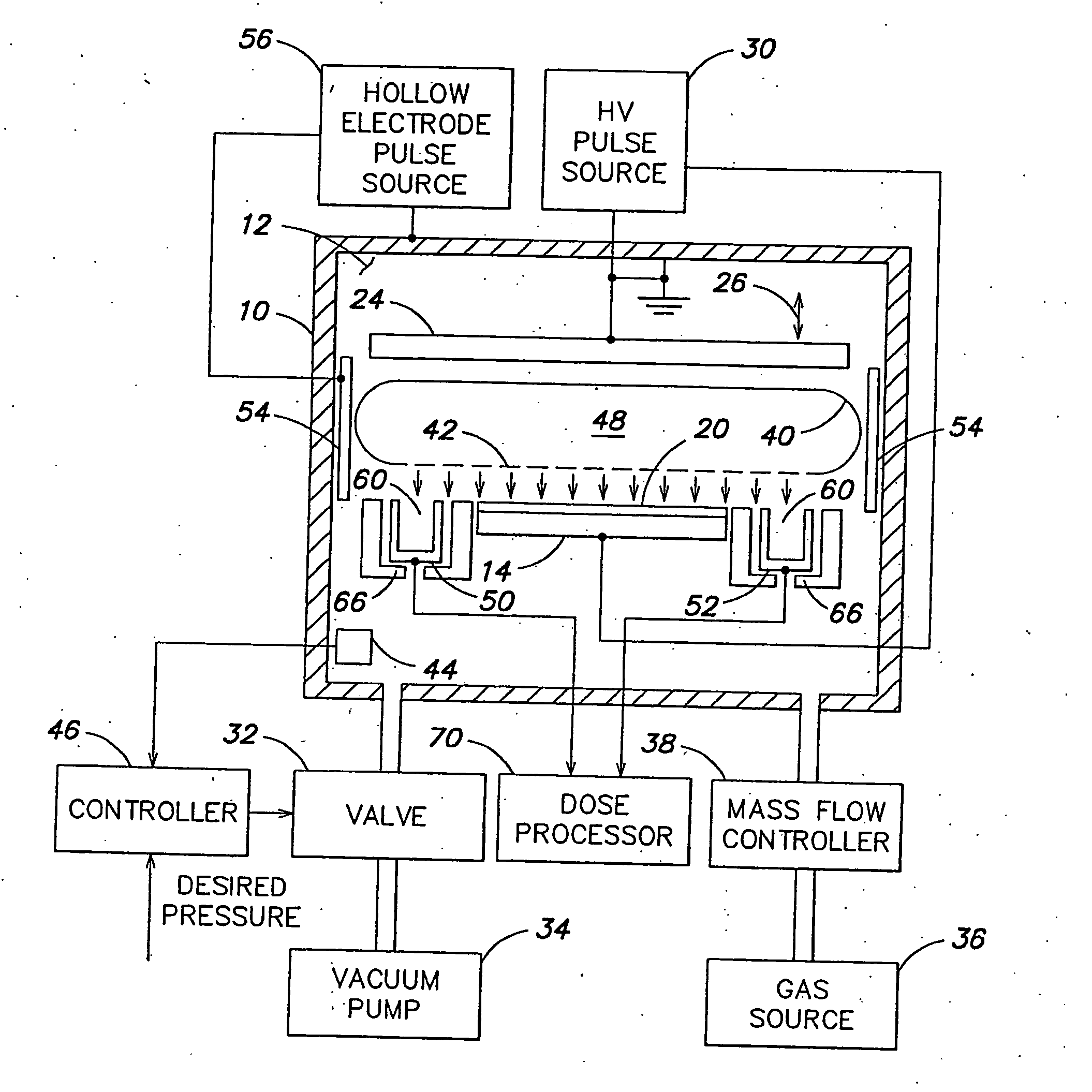
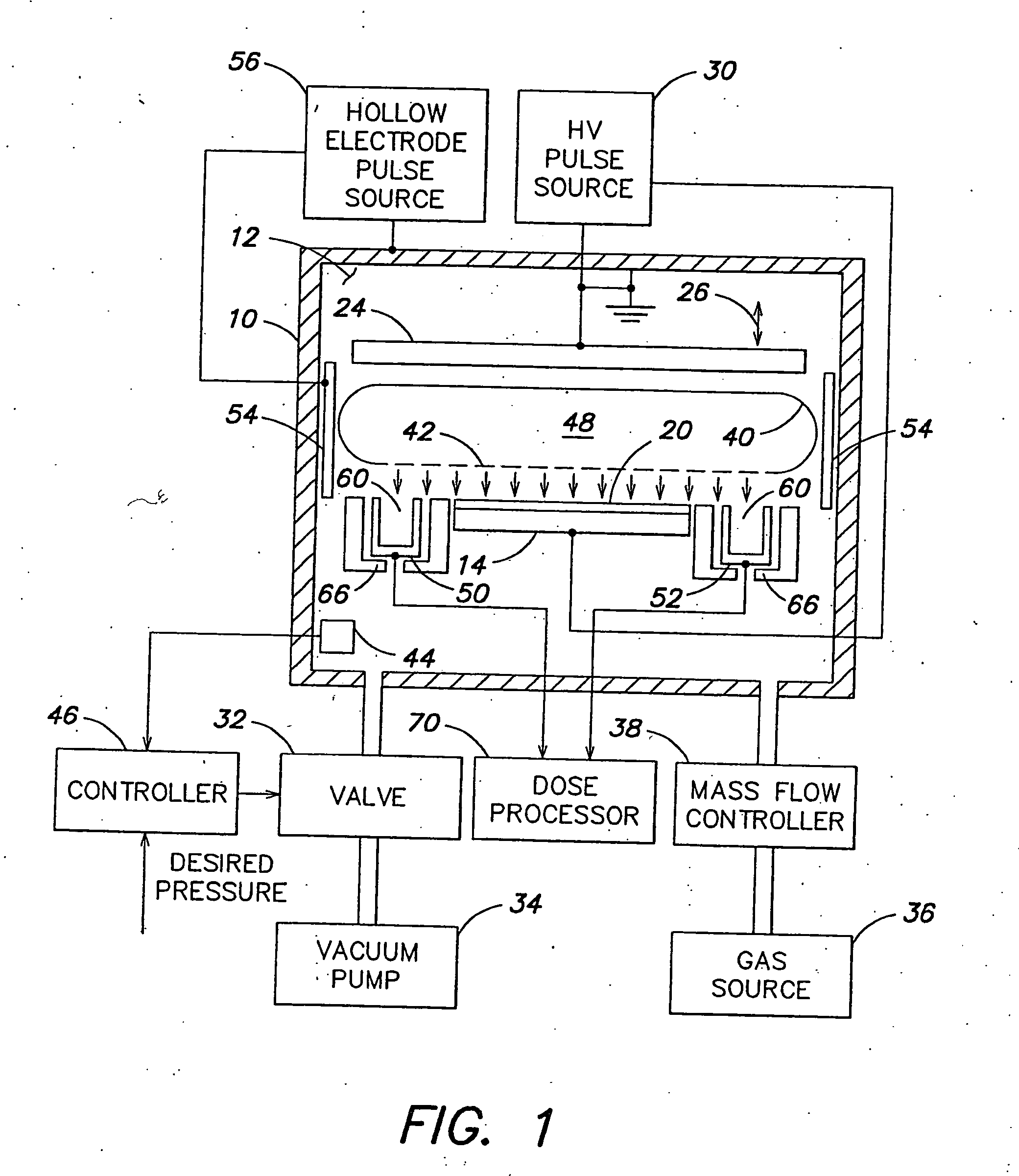
[0015] An example of a plasma ion implantation system suitable for implementation of the present invention is shown schematically in FIG. 1. A process chamber 10 defines an enclosed volume 12. A platen 14 positioned within chamber 10 provides a surface for holding a substrate, such as a semiconductor wafer 20. The wafer 20 may, for example, be clamped at its periphery to a flat surface of platen 14 or may be electrostatically clamped. In one embodiment, the platen has an electrically conductive surface for supporting wafer 20. In another embodiment, the platen includes conductive pins (not shown) for connection to wafer 20. In addition, platen 14 may be equipped with a heating / cooling system to control wafer / substrate temperature.

[0016] An anode 24 is positioned within chamber 10 in spaced relation to platen 14. Anode 24 may be movable in a direction, indicated by arrow 26, perpendicular to platen 14. The anode is typically connected to electrically conductive walls of chamber 10, ...


PUM

PropertyMeasurementUnit
pressureaaaaaaaaaa
pressureaaaaaaaaaa
semi-conductoraaaaaaaaaa

Abstract

Methods and apparatus for plasma implantation of a workpiece, such as a semiconductor wafer, are provided. A method includes introducing into a plasma doping chamber a dopant gas selected from the group consisting of PF3, AsF3, AsF5 and mixtures thereof, forming in the plasma doping chamber a plasma containing ions of the dopant gas, the plasma having a plasma sheath at or near a surface of the workpiece, and accelerating the dopant gas ions across the plasma sheath toward the workpiece, wherein the dopant gas ions are implanted into the workpiece. The selected dopant gas limits deposition of neutral particles on the workpiece.

Description

FIELD OF THE INVENTION [0001] This invention relates to plasma doping systems used for ion implantation of workpieces, such as semiconductor wafers, and, more particularly, to methods and apparatus for limiting deposition of surface layers on semiconductor wafers during plasma implantation. BACKGROUND OF THE INVENTION [0002] Plasma doping systems have been studied for forming shallow junctions in semiconductor wafers and for other applications requiring high current, relatively low energy ions. In a plasma doping system, a semiconductor wafer is placed on a conductive platen, which functions as a cathode and is located in a plasma doping chamber. An ionizable doping gas is introduced into the chamber, and a voltage pulse is applied between the platen and an anode or the chamber walls, causing formation of a plasma containing ions of the dopant gas. The plasma has a plasma sheath in the vicinity of the wafer. The applied pulse causes ions in the plasma to be accelerated across the pl...

Claims


Application Information

Patent Timeline
Patent Type & Authority Applications(United States)
IPC IPC(8): C23C14/00C23C16/00H01L21/31
CPCH01J37/32412H01L21/263H01L21/26506
Inventor WALTHER, STEVEN R.MEHTA, SANDEEPSCHEUER, JAY T.
Owner VARIAN SEMICON EQUIP ASSOC INC
Why Eureka
Try Eureka