Unlock instant, AI-driven research and patent intelligence for your innovation.
Variable gain amplifying circuit with matchable input/output impedance
Inactive Publication Date: 2006-05-11
ALPS ALPINE CO LTD
View PDF13 Cites 3 Cited by
Summary
Abstract
Description
Claims
Application Information
AI Technical Summary
This helps you quickly interpret patents by identifying the three key elements:
Problems solved by technology
Method used
Benefits of technology
Benefits of technology
[0016] According to the variable gain amplifying circuit of the first aspect, the bias voltage of the control electrode of the semiconductor amplifying device is adjusted corresponding to a supplied AGC voltage. In addition, as the amplitude of the input RF signal becomes large, the bias voltage of the control electrode decreases and a main current flowing through the first main electrode and the second main electrode decreases, and thus the signal gain of the semiconductor amplifying device decreases. On the other hand, as the amplitude of the input RF signal becomes small, the bias voltage of the control electrode increases and the main current increases, and thus the signal gain of the semiconductor amplifying device increases. With this configuration, the signal gain of the semiconductor amplifying device is automatically adjusted even the intensity of the electric field of the input RF signal varies. Accordingly, the RF signal has no distortion even when the intensity of the electric field becomes strong. Also, since the RF signal is output from the second main electrode having a low output impedance characteristic of the semiconductor amplifying device, there is an effect in that the output impedance of the variable gain amplifying circuit can approximately match the impedance of an external circuit.
[0017] Further, according to the variable gain amplifying circuit of the second aspect, the bias voltage of each of the control electrodes of the first and second semiconductor amplifying devices is adjusted corresponding to a supplied AGC voltage. In addition, as the amplitude of the input RF signal becomes large, the bias voltage of each of the control electrodes decreases and a main current flowing through the first and second main electrodes of the first and second semiconductor amplifying devices decreases, and thus the signal gains of the first and second semiconductor amplifying devices decrease, respectively. On the other hand, as the amplitude of the input RF signal becomes small, the bias voltage of each of the control electrodes increases and the main current increases, and thus the signal gains of the first and second semiconductor amplifying devices increase, respectively. With this configuration, the signal gains of the firs and second semiconductor amplifying devices are automatically adjusted even the intensity of the electric field of the input RF signal varies. Accordingly, the RF signal has no distortion even when the intensity of the electric field becomes strong. In addition, since the RF signal is supplied to the second main electrode having a low output impedance characteristic of the first semiconductor amplifying device and the RF signal is output from the second main electrode having a low output impedance characteristic of the second semiconductor amplifying device, there is an effect in that the input / output impedance of the variable gain amplifying circuit can match the impedance of an external circuit.
Problems solved by technology
Therefore, it is difficult for the amplification of the RF signal to sufficiently follow the variation of the intensity of the electric field of the RF signal, and signal distortion may occur in some cases.
In addition, since the switching operation on the intensity of the electric field is manually performed, a complicated control operation for switching between the electric field intensities is required to regularly monitor the variation of the intensity of the electric field of the RF signal.
Method used
Image
Click on the blue label to locate the original text in one second.
Reading with bidirectional positioning of images and text.
Examples
first embodiment
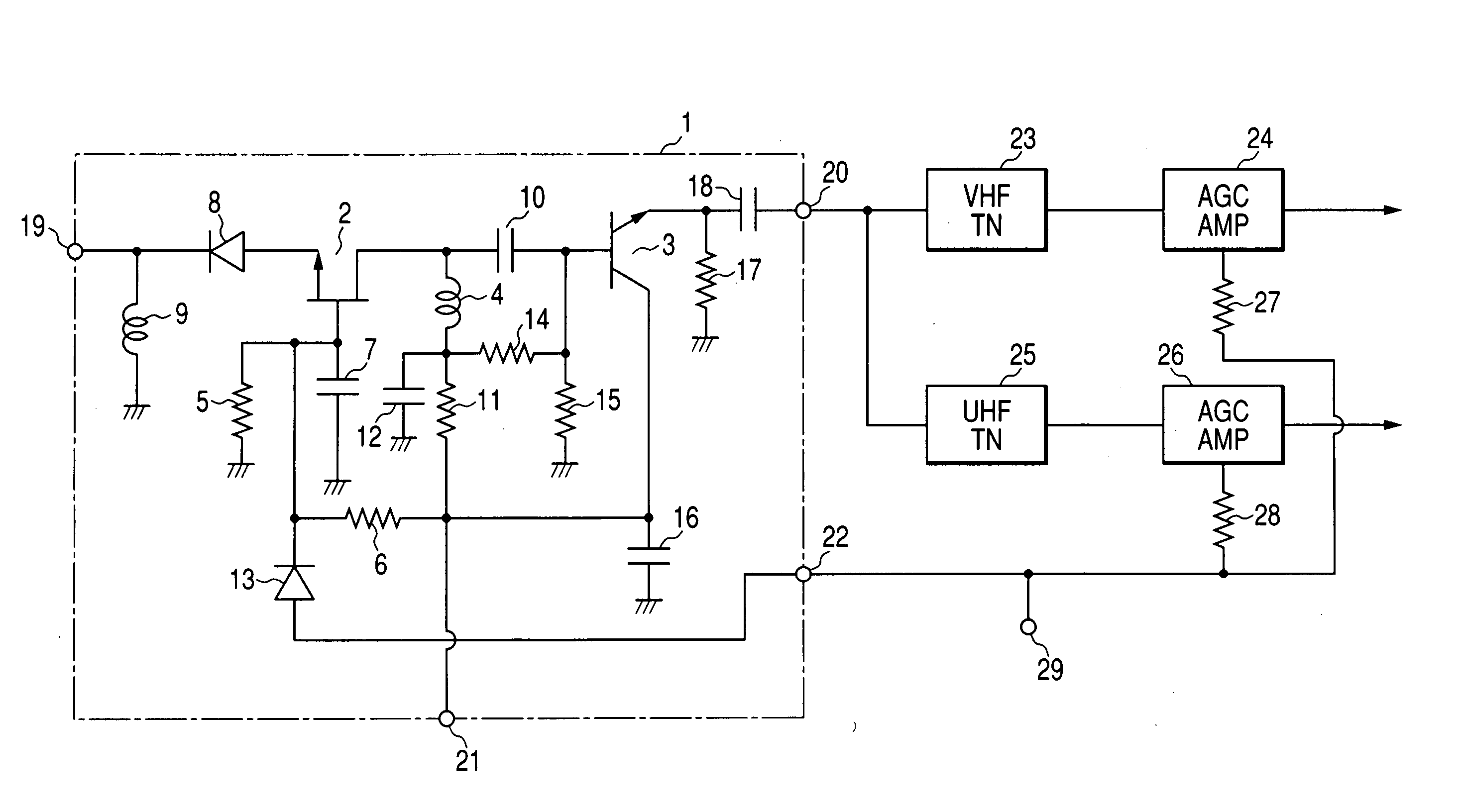
[0022]FIG. 1 is a circuit diagram illustrating an exemplary configuration of a variable gain amplifying circuit, together with a subsequent circuit, according to the invention.
[0023] Referring to FIG. 1, an RF signal amplifying circuit 1 according to the first embodiment includes an FET (first semiconductor amplifying device) 2, a transistor (second semiconductor amplifying device) 3, a drain load inductor 4, gate resistors 5 and 6, a bypass capacitor 7, a PIN diode 8, a shunt inductor 9, a couplingcapacitor 10, a drain resistor (first resistor) 11, a bypass capacitor 12, a diode 13, base voltage dividing resistors (second and third resistors) 14 and 15, a bypass capacitor 16, an emitter load resistor 17, a coupling capacitor 18, an antenna input stage 19, a signal output stage 20, a power supply terminal 21, and an AGC voltage supply stage 22. Further, a subsequent circuit connected to the signal output stage 20 of the variable gain amplifying circuit 1 includes a VHF tuning circu...
second embodiment
[0037]FIG. 2 is a circuit diagram illustrating an exemplary configuration of a variable gain amplifying circuit, together with a subsequent circuit, according to the invention.
[0038] Referring to FIG. 2, a variable gain amplifying circuit 1 according to the second embodiment is different from the variable gain amplifying circuit 1 according to the first embodiment in that the FET 2, the PIN diode 8, and related circuit components are omitted. Specifically, the variable gain amplifying circuit 1 according to the second embodiment includes a transistor (semiconductor amplifying device) 3, a coupling capacitor 10, a bypass capacitor 12, a diode 13, a buffer resistor 13(1), base voltage dividing resistors 14 and 15, a buffer resistor 15(1), a bypass capacitor 16, an emitter load resistor 17, a coupling capacitor 18, an antenna input stage 19, a signal output stage 20, a power supply terminal 21, and an AGC voltage supply stage 22. In addition, a subsequent circuit connected to the signa...
PUM
Abstract
A variable gain amplifying circuit includes a gate-grounded amplifying FET and a collector-grounded amplifying transistor. A gate voltage of the FET and a base voltage of the transistor are adjusted by a supplied AGC voltage. When an input RF signal has small amplitude, the gate voltage is increased by a high AGC voltage so as to increase a main current of the FET, thereby increasing a signalgain of the FET. When the input RF signal has large or medium amplitude, the gate voltage is decreased by a low AGC voltage so as to decrease a main current of the FET, thereby decreasing the signal gain of the FET.
Description
BACKGROUND OF THE INVENTION [0001] 1. Field of the Invention [0002] The present invention relates to a variable gain amplifying circuit which is connected to a front stage of an antenna tuning circuit and has a collector-grounded transistor or a drain-grounded FET for impedance matching at an output stage such that an input RF signal amplified in the transistor or the FET at the output stage has no distortion when the intensity of an electric field of the RF signal is strong. [0003] 2. Description of the Related Art [0004] Conventionally, an RF signal amplifying circuit, which is connected to a front stage of an antenna tuning circuit so as to amplify a received television signal in a television tuner, has been known. The RF signal amplifying circuit has an input stage to which an input adjusting unit is connected so as to correspond to the intensity of an electric-field of an input RF signal, the impedance of the input adjusting unit being adjusted corresponding to the intensity of...
Claims
Application Information
Patent Timeline
Application Date:The date an application was filed.
Publication Date:The date a patent or application was officially published.
First Publication Date:The earliest publication date of a patent with the same application number.
Issue Date:Publication date of the patent grant document.
PCT Entry Date:The Entry date of PCT National Phase.
Estimated Expiry Date:The statutory expiry date of a patent right according to the Patent Law, and it is the longest term of protection that the patent right can achieve without the termination of the patent right due to other reasons(Term extension factor has been taken into account ).
Invalid Date:Actual expiry date is based on effective date or publication date of legal transaction data of invalid patent.

