Cyclic flash memory wear leveling

a flash memory and wear leveling technology, applied in the field of nonvolatile flash memory system operation, can solve the problems of less than optimal wear leveling, erroneous data to be read, storage level shift, etc., and achieve the effect of improving the wear leveling process

Inactive Publication Date: 2006-05-18
SANDISK TECH LLC
View PDF23 Cites 244 Cited by
  • Summary
  • Abstract
  • Description
  • Claims
  • Application Information

AI Technical Summary

Benefits of technology

[0021] According to another aspect of the present invention, experience counts or indications of the usage of individual blocks or groups of blocks may be employed in conjunction with the foregoing to enhance the wear leveling process. This can be worthwhile particularly if the capability of maintaining these counts or indications are being provided in the memory system for other reasons anyway. For example, instead of incrementing through the individual physical blocks in order to designate a block for a wear leveling exchange with an erased pool block, the experience counts of a number of physical blocks within a range of physical block addresses may be examined at one time to select only one or a few of those blocks with the lowest counts to be exchanged while the others of the group are not exchanged. In another example of the use of physical block experience counts, rather than automatically initiating a wear leveling exchange at an interval of a given number of prog

Problems solved by technology

Zones are primarily used to simplify address management such as logical to physical translation, resulting in smaller translation tables, less RAM memory needed to hold these tables, and faster access times to address the currently active region of memory, but because of their restrictive nature can result in less than optimum wear leveling.
These storage levels do shift as a result of charge disturbing programming, reading or erasing operations performed in neighboring or other related memory cells, pages or blocks.
Also, shifting charge levels can be restored back to the centers of their state ranges from time-to-time, before disturbing operations cause them to shift completely out of their defined ranges and thus cause erroneous data to be read.
This is thought to be t

Method used


Image

  • Cyclic flash memory wear leveling
  • Cyclic flash memory wear leveling
  • Cyclic flash memory wear leveling

Examples


Embodiment Construction

Memory Architectures and Their Operation

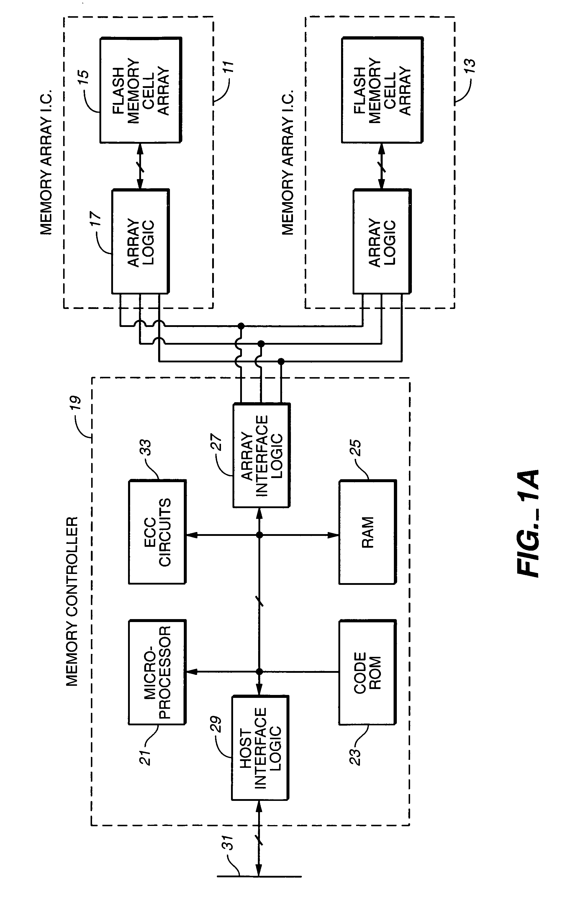
[0037] Referring initially to FIG. 1A, a flash memory includes a memory cell array and a controller. In the example shown, two integrated circuit devices (chips) 11 and 13 include an array 15 of memory cells and various logic circuits 17. The logic circuits 17 interface with a controller 19 on a separate chip through data, command and status circuits, and also provide addressing, data transfer and sensing, and other support to the array 13. A number of memory array chips can be from one to many, depending upon the storage capacity provided. The controller and part or the entire array can alternatively be combined onto a single integrated circuit chip but this is currently not an economical alternative.

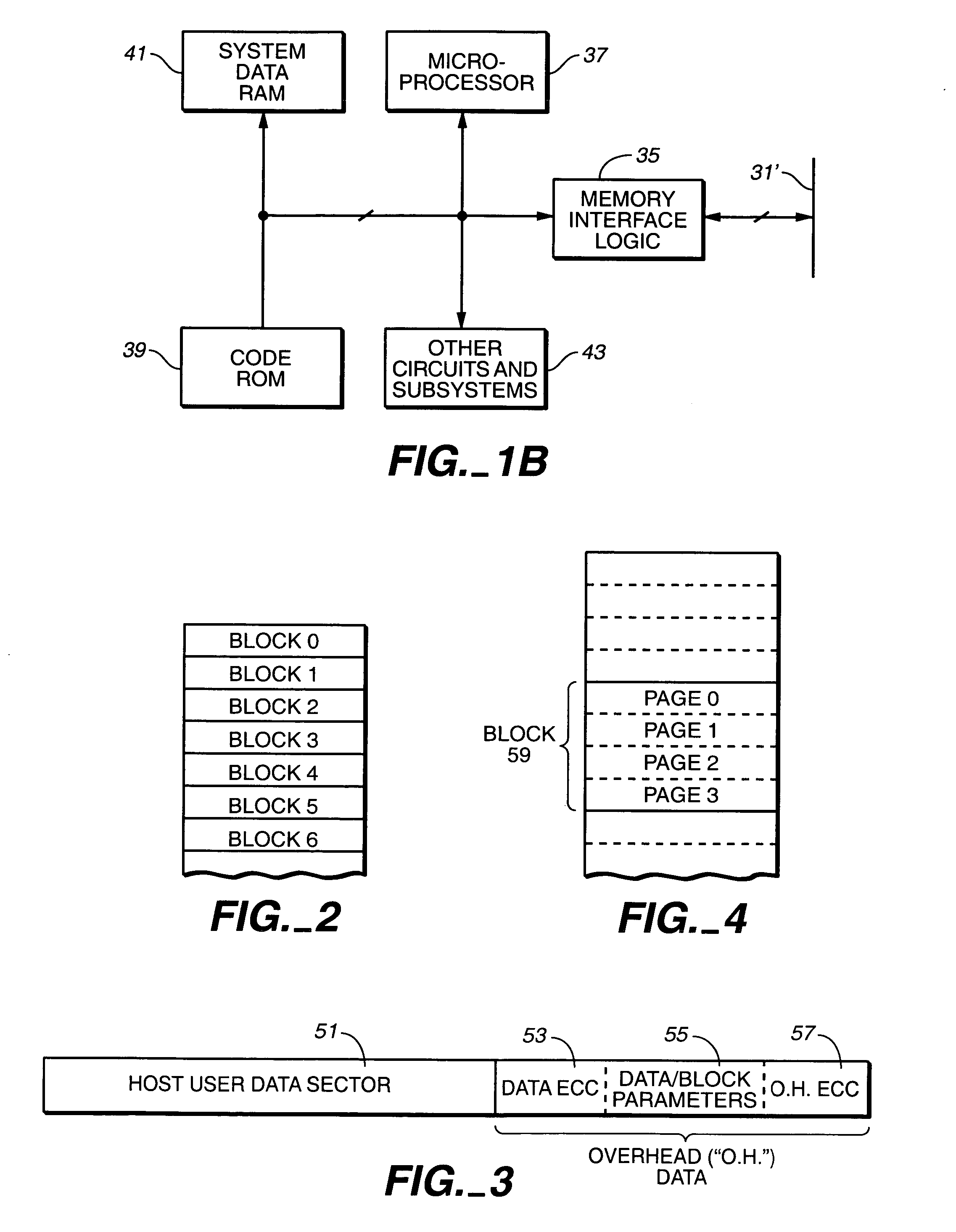
[0038] A typical controller 19 includes a microprocessor 21, a read-only-memory (ROM) 23 primarily to store firmware and a buffer memory (RAM) 25 primarily for the temporary storage of user data either being written to or read from the memory ...


PUM


Abstract

A re-programmable non-volatile memory system, such as a flash EEPROM system, having its memory cells grouped into blocks of cells that are simultaneously erasable is operated in a manner to level out the wear of the individual blocks through repetitive erasing and re-programming. This may be accomplished without use of counts of the number of times the individual blocks experience erase and re-programming but such counts can optionally aid in carrying out the wear leveling process. Individual active physical blocks are chosen to be exchanged with those of an erased block pool in a predefined order.

Description

BACKGROUND AND SUMMARY OF RELATED PATENTS AND APPLICATIONS [0001] This invention relates generally to the operation of non-volatile flash memory systems, and, more specifically, to techniques of even usage among different blocks or other portions of the memory, particularly in memory systems having large memory cell blocks. [0002] There are many commercially successful non-volatile memory products being used today, particularly in the form of small form factor cards, which employ an array of flash EEPROM (Electrically Erasable and Programmable Read Only Memory) cells formed on one or more integrated circuit chips. A memory controller, usually but not necessarily on a separate integrated circuit chip, interfaces with a host to which the card is removably connected and controls operation of the memory array within the card. Such a controller typically includes a microprocessor, some non-volatile read-only-memory (ROM), a volatile random-access-memory (RAM) and one or more special circ...

Claims


Application Information

Patent Timeline
IPC IPC(8): G06F12/00
CPCG06F12/0246G06F2212/1036G06F2212/7211
Inventor GOROBETS, SERGEY A.BENNETT, ALAN D.SMITH, PETER J.SINCLAIR, ALAN W.CONLEY, KEVIN M.ROYALL, PHILIP D.
Owner SANDISK TECH LLC
Why Eureka
Try Eureka