Supercharge Your Innovation With Domain-Expert AI Agents!

Method for manufacturing printed wiring board

a printing method and wiring board technology, applied in the direction of printed circuit parts, non-metallic protective coating applications, chemistry apparatus and processes, etc., can solve the problems of difficult force into spaces, voids to be produced in subsequent processing, and uneven and adequate resin layer formation, etc., to facilitate the thin spreading of resin layer and facilitate polishing

Inactive Publication Date: 2006-06-01
NODA SCREEN
View PDF2 Cites 1 Cited by
  • Summary
  • Abstract
  • Description
  • Claims
  • Application Information

AI Technical Summary

Benefits of technology

[0009] According to the present invention, since the resin layer is pressed, even if the resin layer is gradually raised at a part where the circuit patterns are formed thereunder, the raised part is compressed so that the resin layer as a whole is made to thinly and evenly spread. Even if sparse and dense parts are present in the circuit patterns on the substrate, a semi-cured resin sheet with resin patterns complementary to the circuit patterns may be created beforehand. The resin patterns are located on the surface of the semi-cured resin sheet facing the circuit patterns, so that the resin layer as a whole is made to be substantially uniform regardless of the sparse and dense state of the circuit patterns. Since only a relatively thin resin layer remains on the circuit patterns when the resin is cured in this state, it is possible to obtain a substantially flat substrate with the circuit patterns exposed by polishing the circuit patterns at a strength that will not damage the circuit patterns.
[0010] In the case of the substrate having through holes, locating additional resin beforehand at the positions of the semi-cured resin sheet corresponding to the through holes allows the entire resin layer on the substrate to be uniformly formed without causing a deficiency of resin proximate to the through holes.
[0012] Further, the metallic foil with a roughened surface facing the resin layer facilitates the thin spreading of the resin layer when the metallic foil is superposed on the resin layer prior to the time of the pressing of the resin layer. The surface of the resin layer is also formed in a fine uneven state corresponding to the roughened surface of the metallic foil. As a result, the residual resin layer can be more easily polished.
[0013] Further, in the case where the above described metallic foil is formed with a metal of a different kind than the metal used for the circuit patterns, the metallic foil can be removed by selective etching or dissolving only the metallic foil, without affecting the metal of the circuit patterns.

Problems solved by technology

However, the circuit pattern of a printed board, which may be manufactured by a subtractive method for removing unnecessary amounts of copper foil via etching, is generally formed into an uneven configuration in which the circuit pattern portion is slightly raised above the surrounding surface of the base material.
However, the resin layer may not be formed uniformly and adequately because of the presence of sparse or dense sections of circuit patterns on the substrate, and the presence or absence of through holes, etc.
For example, in the sections where the circuit patterns are dense, the resin sheet tends to be difficult to force into spaces between the circuit patterns.
As a result, the remaining unfilled spaces may cause voids to be produced in subsequent processing.
In addition, considerably thick resin may remain on top of the circuit patterns and cause the surface of the resin layer to become uneven.
On the contrary, in the areas where the circuit patterns are sparse and where through holes are formed, the amount of resin may be insufficient as compared with other areas of the printed wiring board.
In such a situation, the resin layer is hardly uniformly formed across the whole surface, even after having been pressed via a smoothing plate.
A substrate having such gradually rising and falling sections can also be difficult to polish accurately and flatly.

Method used


Image

  • Method for manufacturing printed wiring board
  • Method for manufacturing printed wiring board
  • Method for manufacturing printed wiring board

Examples


Embodiment Construction

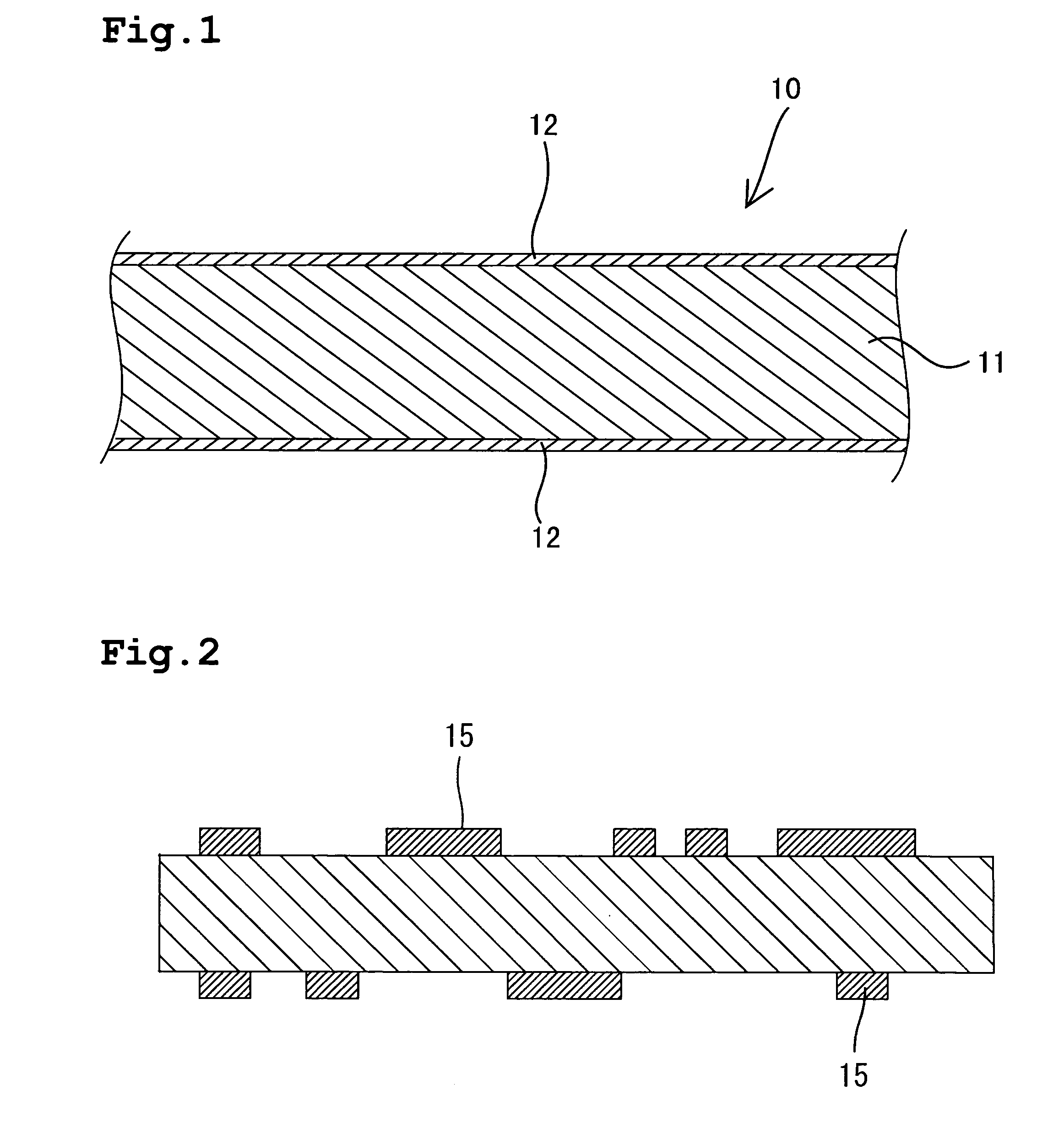
[0029] In the present embodiment, as shown in FIG. 1, a copper clad laminated board 10 with copper foils 12 adhered to both sides of a glass epoxy substrate 11 having a thickness of, for example, 100 μm to 3000 μm is used as a base material. Circuit patterns 15 are formed on the copper clad laminated board 10 by a known photo etching method (see FIG. 2).

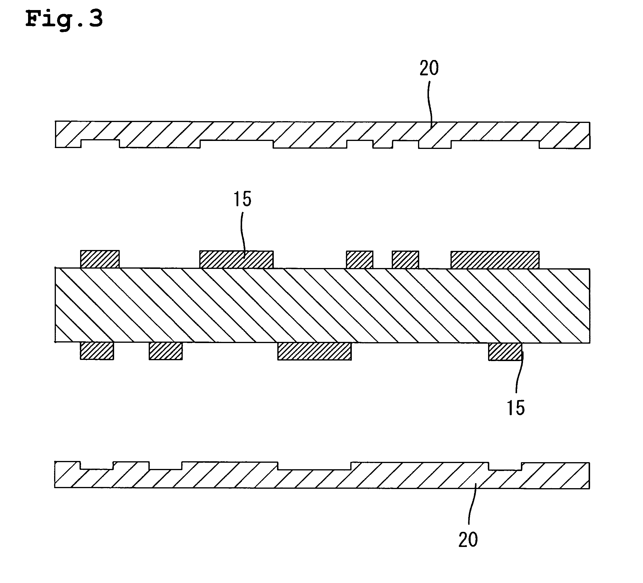
[0030] As shown in FIGS. 3 and 4, resin layers 16 (FIG. 4) are formed on the surfaces of the substrate by laminating resin sheets 20 with a thickness of about 30 μm onto the circuit patterns 15 of the wiring board. The resin sheets 20 may be formed of e.g., semi-cured thermosetting epoxy resin. Thermosetting epoxy resin having resin patterns complementary to the circuit patterns 15 are formed beforehand on the surface of the resin sheets 20 facing the circuit patterns 15.

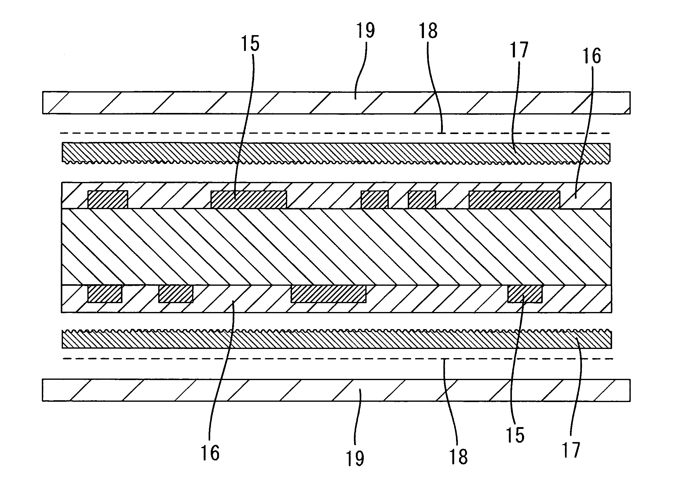
[0031] As shown in FIG. 4, nickel foils 17, with a thickness of 18 μm and one face of which is roughened by a needle shaped plating, are placed on the resin layers...


PUM

PropertyMeasurementUnit
thicknessaaaaaaaaaa
thicknessaaaaaaaaaa
thicknessaaaaaaaaaa

Abstract

There is provided a method for manufacturing a printed wiring board, including the following steps. Forming a resin layer on a printed wiring board with circuit patterns formed thereon wherein the resin layer is formed by superposing a semi-cured resin sheet, in which patterns complementary to the circuit patterns are included on a surface of the resin sheet facing the circuit patterns. Pressing and forcing the resin layer into spaces between the circuit patterns and curing the resin layer. And then polishing the cured resin covering said circuit patterns, thereby exposing said circuit patterns.

Description

TECHNICAL FIELD [0001] The present invention relates to a method for manufacturing a printed wiring board of which the surface of the board is flattened. BACKGROUND ART [0002] In the case of manufacturing a multi-layer printed wiring board by e.g. a build-up method, it is necessary to flatten the surfaces of a lower layer substrate in order to increase the wiring density of the assembly. However, the circuit pattern of a printed board, which may be manufactured by a subtractive method for removing unnecessary amounts of copper foil via etching, is generally formed into an uneven configuration in which the circuit pattern portion is slightly raised above the surrounding surface of the base material. [0003] Therefore, in order to flatten a printed board containing a surface formed into an uneven form as described above, the following method has been proposed. For example, there has been proposed a method comprising the steps of: laminating a semi-cured resin sheet onto circuit pattern...

Claims


Application Information

Patent Timeline
Patent Type & Authority Applications(United States)
IPC IPC(8): B29C65/00H05K3/00H05K3/22H05K3/28H05K3/46
CPCH05K3/0094H05K3/281H05K2201/09036H05K2201/0959H05K2201/09881H05K2203/0108H05K2203/025H05K2203/0278H05K2203/1152H05K3/28H05K3/22H05K3/46
Inventor MURAKAMI, KEIICHI
Owner NODA SCREEN
Features
  • R&D
  • Intellectual Property
  • Life Sciences
  • Materials
  • Tech Scout
  • Unparalleled Data Quality
  • Higher Quality Content
  • 60% Fewer Hallucinations
Learn More