

Aqueous dispersion for chemical mechanical polishing and chemical mechanical polishing method
a technology of chemical mechanical polishing and aqueous dispersion, which is applied in the direction of electrical equipment, chemistry apparatus and processes, other chemical processes, etc., can solve the problems of limited effect achieved by the polishing method, difficulty in implementing a state, and high polishing rate, so as to reduce the polishing rate and achieve high polishing rate , the effect of high flatness
- Summary
- Abstract
- Description
- Claims
- Application Information
AI Technical Summary
Benefits of technology
Problems solved by technology
Method used
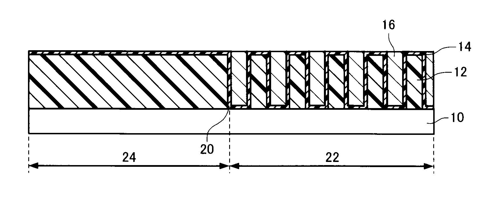
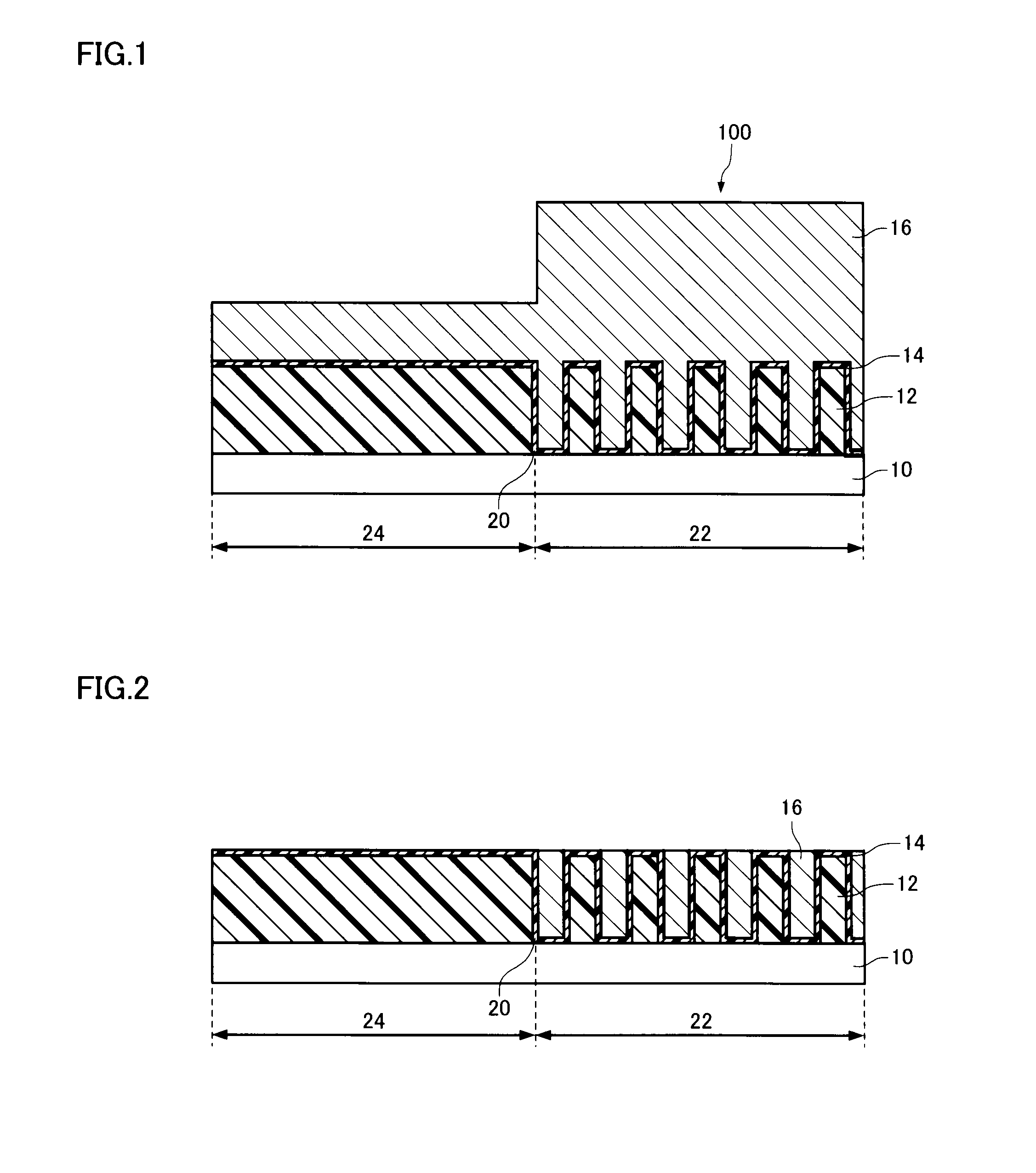
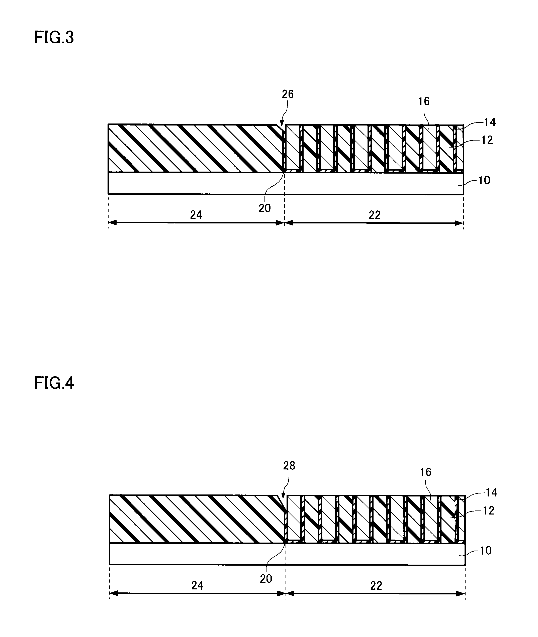
Image

Examples
experimental example 1
4.4 Experimental Example 1
4.4.1 Unpatterned Substrate Polishing Evaluation
[0231]A porous polyurethane polishing pad (“IC1000” manufactured by Nitta Haas Inc.) was installed in a chemical mechanical polishing apparatus (“EPO112” manufactured by Ebara Corporation). A polishing rate measurement substrate was polished for 1 minute under the following polishing conditions while supplying one of the chemical mechanical polishing aqueous dispersions S1 to S11. The polishing rate and wafer contamination were evaluated by the following methods. The results are shown in Tables 3 and 4.
4.4.1a Measurement of Polishing Rate
[0232](1) Polishing Rate Measurement Substrate
[0233]8-inch silicon substrate with thermal oxide film on which a copper film having a thickness of 15,000 angstroms was stacked
[0234]8-inch silicon substrate with a thermal oxide film on which a tantalum film having a thickness of 2000 angstroms was stacked
[0235]8-inch silicon substrate on which a low-dielectric-constant insulatin...
experimental example 2
4.5 Experimental Example 2
4.5.1 Unpatterned Substrate Polishing Evaluation
[0277]A porous polyurethane polishing pad (“IC1000” manufactured by Nitta Haas Inc.) was installed in a chemical mechanical polishing apparatus (“EPO112” manufactured by Ebara Corporation). A polishing rate measurement substrate was polished for 1 minute under the following polishing conditions while supplying one of the chemical mechanical polishing aqueous dispersions S12 to S41. The polishing rate and wafer contamination were evaluated by the following methods. The results are shown in Tables 5 to 8.
4.5.1a Measurement of Polishing Rate
[0278](1) Polishing Rate Measurement Substrate
[0279]8-inch silicon substrate with thermal oxide film on which a copper film having a thickness of 15,000 angstroms was stacked
[0280]8-inch silicon substrate with a thermal oxide film on which a tantalum film having a thickness of 2000 angstroms was stacked
[0281](2) Polishing Conditions
[0282]Head rotational speed: 70 rpm
[0283]Head...
PUM
| Property | Measurement | Unit |
|---|---|---|
| pKa | aaaaa | aaaaa |
| particle diameter | aaaaa | aaaaa |
| pH | aaaaa | aaaaa |
Abstract
Description
Claims
Application Information