Tools for polishing and associated methods

a technology of tools and slurry, applied in the field of polishing tools, can solve the problems of accumulating polishing debris coming from the workpiece, abrasive slurry, pad dresser, etc., and achieve the effect of facilitating polishing

Active Publication Date: 2007-07-10
KINIK
View PDF7 Cites 33 Cited by
  • Summary
  • Abstract
  • Description
  • Claims
  • Application Information

AI Technical Summary

Benefits of technology

[0015]Additionally, the polishing tool may be substantially solid metal or it may contain various proportions of metal material within the solid substrate. For example, in one aspect, the polishing tool may be comprised of at least about 50% metal. In another aspect, the polishing tool may be comprised of at least about 75% metal. In yet another aspect, the polishing tool may be comprised of at least about 95% metal. One useful metal may include Al, and as such the polishing tool may be substantially solid aluminum, or it may be an alloy thereof. For example, one useful alloy may include Al—Si. One benefit of utilizing metal polishing tools is the capability to introduce an electrical bias in the tool to facilitate polishing by electrolytic reactions.

Problems solved by technology

One problem that arises with regard to maintaining the pad surface, however, is an accumulation of polishing debris coming from the work piece, the abrasive slurry, and the pad dresser.
This accumulation causes a “glazing” or hardening of the top of the pad, mats the fibers down, and thus makes the pad surface less able to hold the abrasive particles of the slurry.
These effects significantly decrease the pad's overall polishing performance.
Further, with many pads, the pores used to hold the slurry, become clogged, and the overall asperity of the pad's polishing surface becomes depressed and matted.
As semiconductor technology continues toward size reduction to the nano-scale, however, current CMP polishing techniques are proving to be inadequate.
With such a reduction in scale, materials utilized to construct circuit elements have become more delicate, both in size and materials.
There are a number of problems associated with modifying current CMP processes to accommodate such delicate polishing.
Generally speaking, the superabrasive particles are so small that a traditional metal matrix is often unsuitable for holding and retaining them.
However, such a variation would render a dresser useless if it were required to dress a CMP pad and achieve polishing of extremely small and delicate circuit elements.
The highest asperities exert the highest pressure, and would thus scratch and damage the wafer.
In addition to drastic height variations relative to the delicacy of the polishing operation, damage to the wafer can also occur due to the abrasive particles themselves.
Sizing of these particles can be problematic, particularly with the smaller sizes required for more delicate polishing operations.
Larger abrasive particles that tend to cause surface damage to the wafer are thus difficult to eliminate from the slurry.

Method used


Image

  • Tools for polishing and associated methods
  • Tools for polishing and associated methods
  • Tools for polishing and associated methods

Examples


example 1

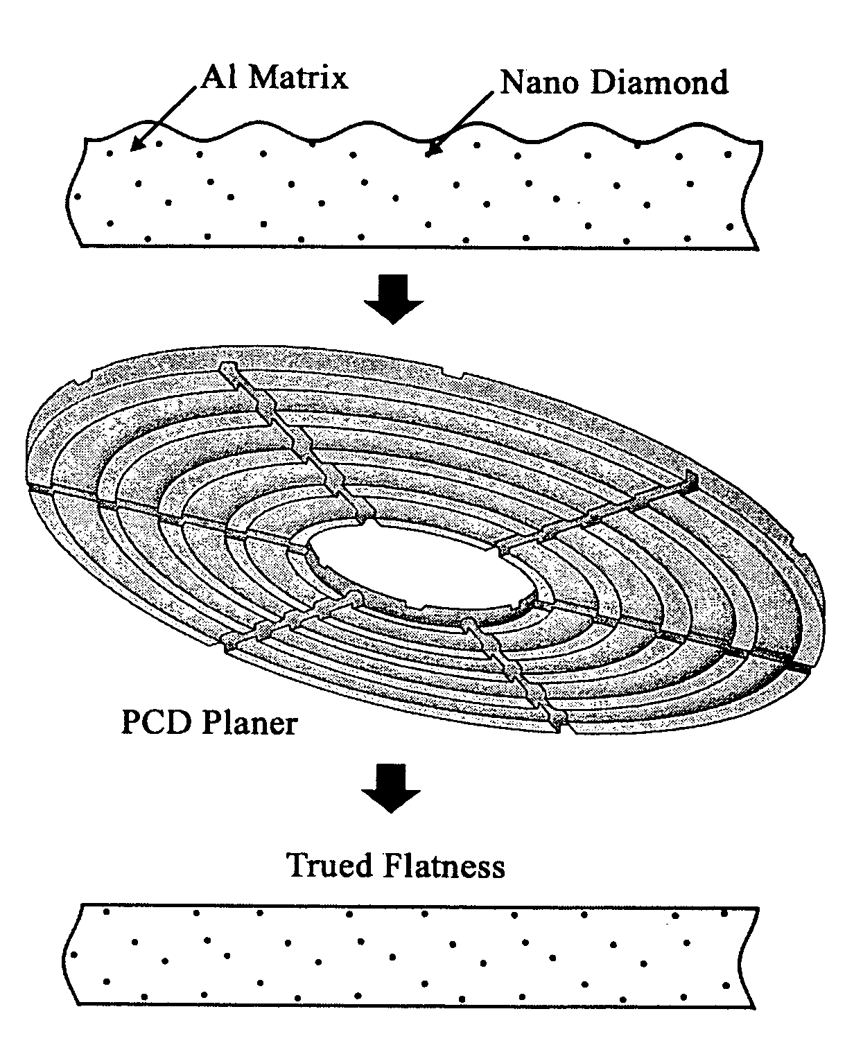
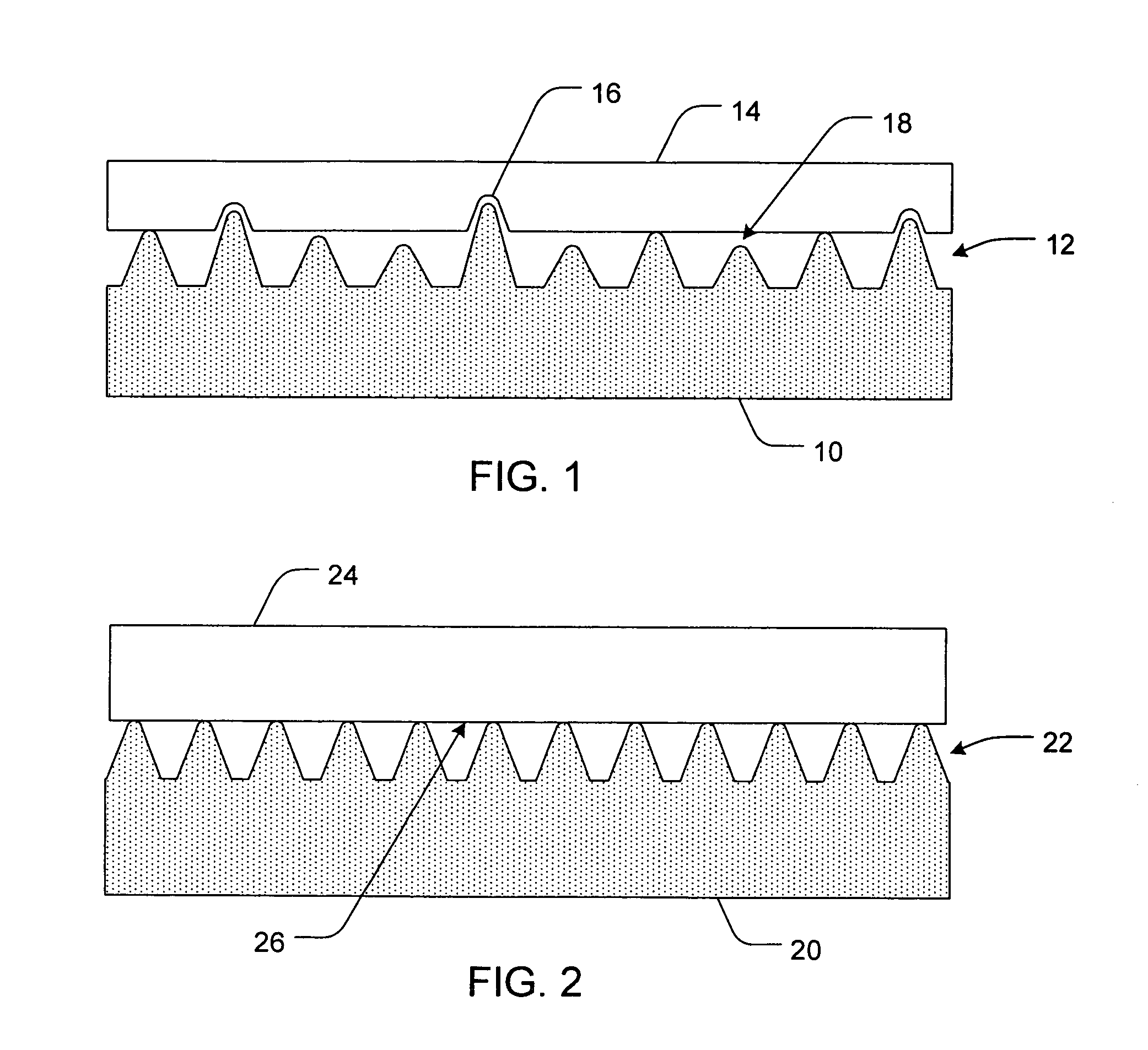
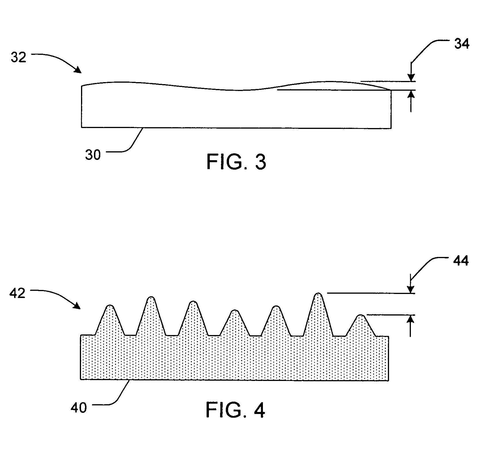
[0071]Nano diamond particles of Tomei PM powder (50 nm) are mixed in with Al powder and melted in vacuum to form a mixture. The mixture is diluted with agitation in a pool of molten Al—Si alloy under protected atmosphere. The resulting alloy is cast to form a thin flat layer that is rolled to a uniform thickness. The layer is then cut to form a circular disk. The disk is mounted on a rotating platen and trued with a PCD planer to a roughness (RA) of less than 5 microns. FIG. 5 shows a depiction of a starting surface (top), a PCD planer (middle), and a final trued surface (bottom). A PCD dresser is used to create uniform asperities of about 10 microns. FIG. 6 shows a depiction of a starting surface (top), a PCD dresser (middle), and a dressed surface (bottom). This textured pad is used to polish a silicon wafer to a mirror finish of 3 nm RA.

example 2

[0072]A stainless steel sheet is flattened and mounted on a rotating platen. The surface is trued with a PCD planer and subsequently dressed with a PCD dresser to create uniform asperities of about 10 microns. This textured steel pad is used to polish a copper coated print circuit board to achieve mirror finish of 1 micron RA.


PUM

PropertyMeasurementUnit
surface roughness RAaaaaaaaaaa
RAaaaaaaaaaa
RAaaaaaaaaaa

Abstract

Polishing tools and associated methods are disclosed. In one aspect, a method of polishing a work piece is provided. Such a method may include providing a polishing tool having asperities on a working surface, where the asperities have a tip-to-tip RA value of less than or equal to about 10 μm, and the working surface has a surface roughness RA value of less than or equal to about 50 μm. The method may further include contacting the tips of the asperities against an interface surface of the work piece and moving the tips of the asperities in a direction substantially parallel to the interface surface of the work piece such that the interface surface is polished.

Description

FIELD OF THE INVENTION[0001]The present invention relates generally to polishing tools and associated methods. Accordingly, the present invention involves the chemical and material science fields.BACKGROUND OF THE INVENTION[0002]Many industries utilize various types of mechanical polishing processes for polishing work pieces. For example, the computer manufacturing industry relies heavily on chemical mechanical polishing (CMP) processes for polishing wafers of ceramics, silicon, glass, quartz, and metals. Such polishing processes generally entail applying the wafer against a rotating pad made from a durable organic substance such as polyurethane. A chemical slurry is utilized that contains a chemical capable of breaking down the wafer substance and an amount of abrasive particles which act to physically erode the wafer surface. The slurry is continually added to the rotating CMP pad, and the dual chemical and mechanical forces exerted on the wafer cause it to be polished in a desire...

Claims


Application Information

Patent Timeline
Patent Type & Authority Patents(United States)
IPC IPC(8): B24B1/00
CPCB24B7/228B24B37/26B24B53/017B24D3/06
Inventor SUNG, CHIEN-MIN
Owner KINIK
Why Eureka
Try Eureka