Dark current reduction circuitry for CMOS active pixel sensors

a technology of dark current reduction and active pixel sensors, which is applied in the field of complementary metal oxide semiconductor (cmos) active pixel sensors, can solve the problems of inherently and negatively affecting the imaging process, increasing the cost of manufacturing image sensor circuits, etc., and achieves the effect of reducing gidl

Inactive Publication Date: 2006-06-01
APTINA IMAGING CORP
View PDF5 Cites 5 Cited by
  • Summary
  • Abstract
  • Description
  • Claims
  • Application Information

AI Technical Summary

Benefits of technology

[0011] The present invention provides a row driver circuit for supplying reset voltage levels to a plurality of reset transistors of an active pixel sensor array while minimizing gate induced drain leakage (GIDL). The row driver circuit is configured to supply a high voltage level (e.g., Vdd or higher) to the reset transistors of the array during a reset operation. The row driver circuit is further configured to supply a low voltage level that is lower than the high voltage level but higher than a ground level voltage, to the reset transistors of the array when the pixels are not being reset (e.g., during integration). The reduced potential difference between the respective gates of the reset transistors and the respective photodiodes of the pixels, when the pixels are not being reset, results in reduced GIDL.

Problems solved by technology

Doing so, however, particularly for a CMOS imager pixel, can require deviating from a standard MOS integrated circuit fabrication process, thereby further increasing the cost of manufacturing the image sensor circuit.
One problem commonly encountered with the pixel reset process is that of leakage current flowing from the reset voltage source (e.g., Vdd of FIG. 1) through the reset transistor 104 and to the photodiode 106 when the reset transistor 104 is not activated (e.g., the RST signal is set to ground).
The introduction of such leakage current, known as gate induced drain leakage (GIDL), and which is a prominent component of pixel noise known as “dark current,” inherently and negatively effects the imaging process.

Method used


Image

  • Dark current reduction circuitry for CMOS active pixel sensors
  • Dark current reduction circuitry for CMOS active pixel sensors
  • Dark current reduction circuitry for CMOS active pixel sensors

Examples


Embodiment Construction

[0024] In the following detailed description, reference is made to the accompanying drawings which form a part hereof, and in which is shown by way of illustration specific embodiments in which the invention may be practiced. These embodiments are described in sufficient detail to enable those of ordinary skill in the art to make and use the invention, and it is to be understood that structural, logical or procedural changes may be made to the specific embodiments disclosed without departing from the spirit and scope of the present invention.

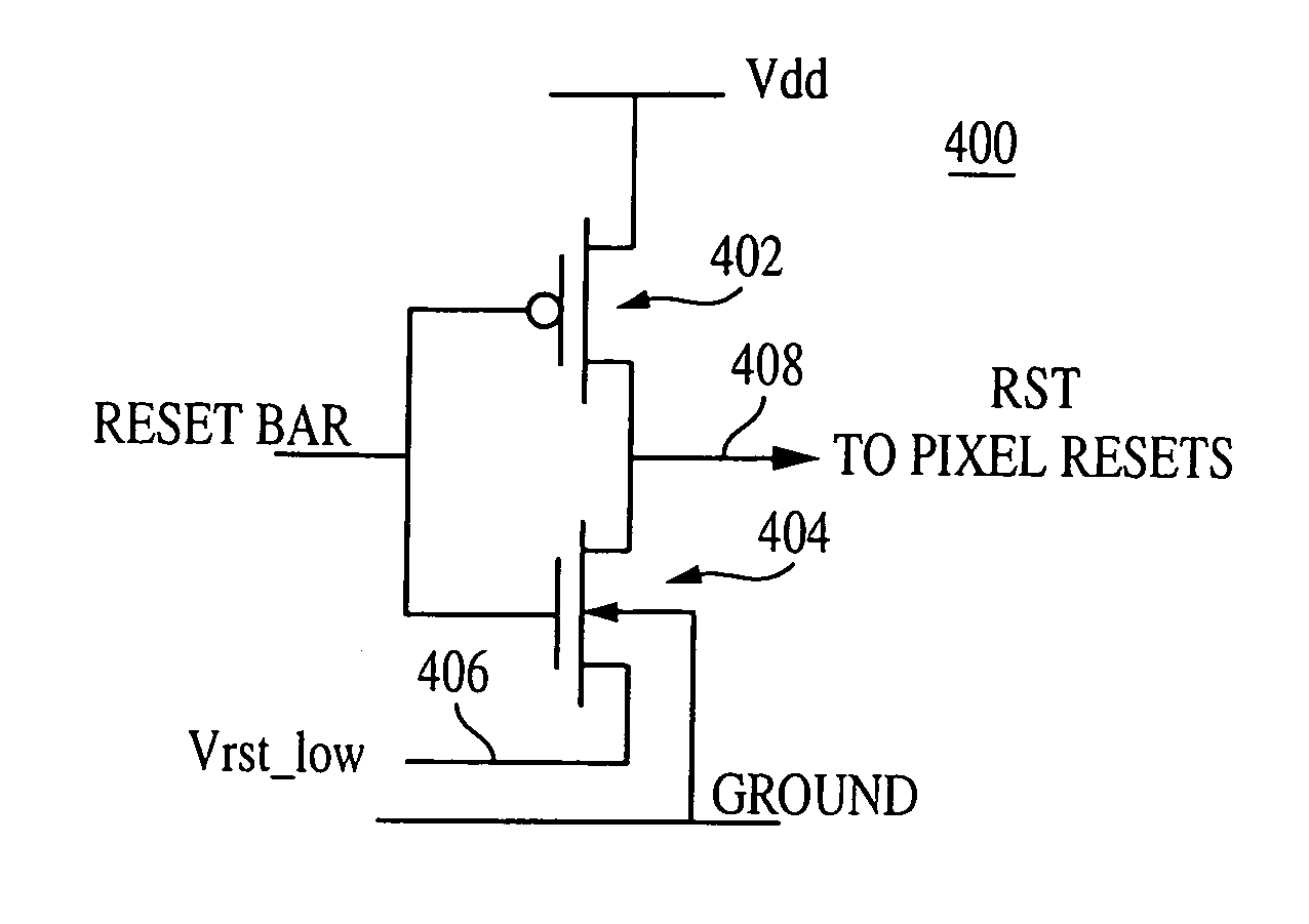
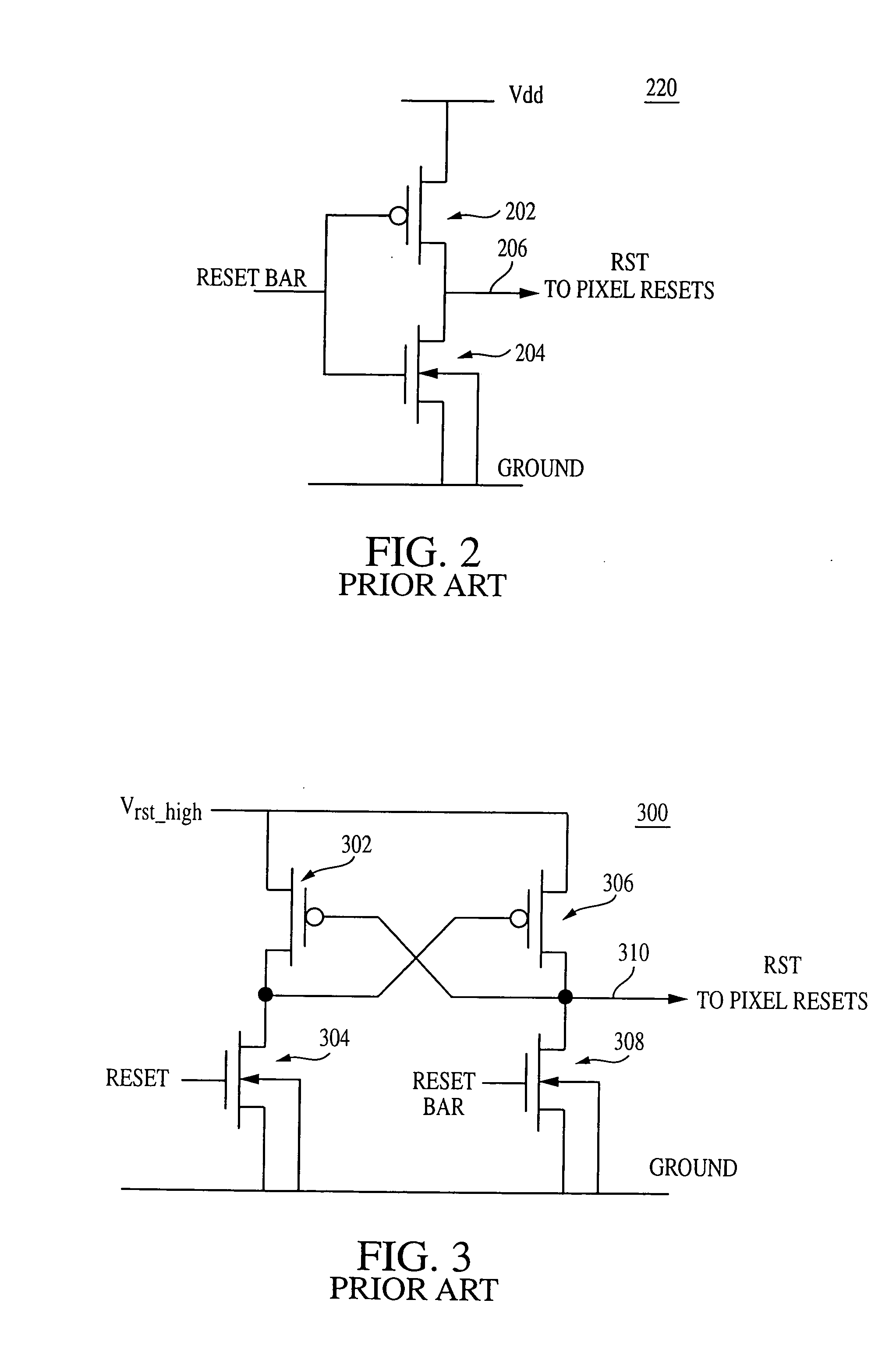
[0025]FIG. 4 depicts a schematic diagram of a row driver circuit 400, in accordance with an exemplary embodiment of the invention. The row driver circuit 400 generates the RST signal applied to the gate of a reset transistor (e.g., 104 of FIG. 1). Similarly to the row driver circuit 200 of FIG. 2, the row driver circuit 400 has two transistors 402, 404 configured as an inverter. The operation of row driver circuit 400 is identical to that of ro...


PUM


Abstract

A row driver circuit is disclosed for supplying a reset voltage to a plurality of reset transistors of an active pixel sensor array while minimizing gate induced drain leakage (GIDL). The row driver circuit is configured to supply a high voltage level (e.g., Vdd or higher) to the reset transistors of the array during a reset operation. The row driver circuit is further configured to supply a low voltage level (e.g., a voltage level higher than ground) to the reset transistors of the array when the pixels are not being reset (e.g., during integration). The reduced potential difference realized between the respective gates of the reset transistors and the respective photodiodes of the pixels, when the pixels are not being reset, results in reduced GIDL.

Description

FIELD OF THE INVENTION [0001] The present invention relates generally to complementary metal oxide semiconductor (CMOS) active pixel sensors, and more particularly to the reduction of dark current in CMOS active pixel sensors. BACKGROUND OF THE INVENTION [0002] Image sensor circuits are used in a variety of different types of digital image capture systems, including products such as scanners, copiers, and digital cameras. The image sensor is typically composed of an array of light-sensitive pixels that are electrically responsive to incident light reflected from an object or scene whose image is to be captured. [0003] The performance of an image capture system depends in large part on the sensitivity of each individual pixel in the sensor array and its immunity from noise. Pixel sensitivity is defined here as being related to the ratio of a change in the pixel output voltage to the photogenerated charge in the pixel. Noise here is defined as small fluctuations in a signal that can b...

Claims


Application Information

Patent Timeline
Patent Type & Authority Applications(United States)
IPC IPC(8): H01L27/00H04N3/15
CPCH04N3/1568H04N5/363H04N5/3698H04N5/374H04N25/65H04N25/709H04N25/76
Inventor BARNA, SANDOR L.
Owner APTINA IMAGING CORP
Why Eureka
Try Eureka