Charge trapping dielectric structure for non-volatile memory
- Summary
- Abstract
- Description
- Claims
- Application Information
AI Technical Summary
Benefits of technology
Problems solved by technology
Method used
Image


Examples
Embodiment Construction
[0021] A detailed description of embodiments of the present invention is provided with reference to the FIGS. 1-9.
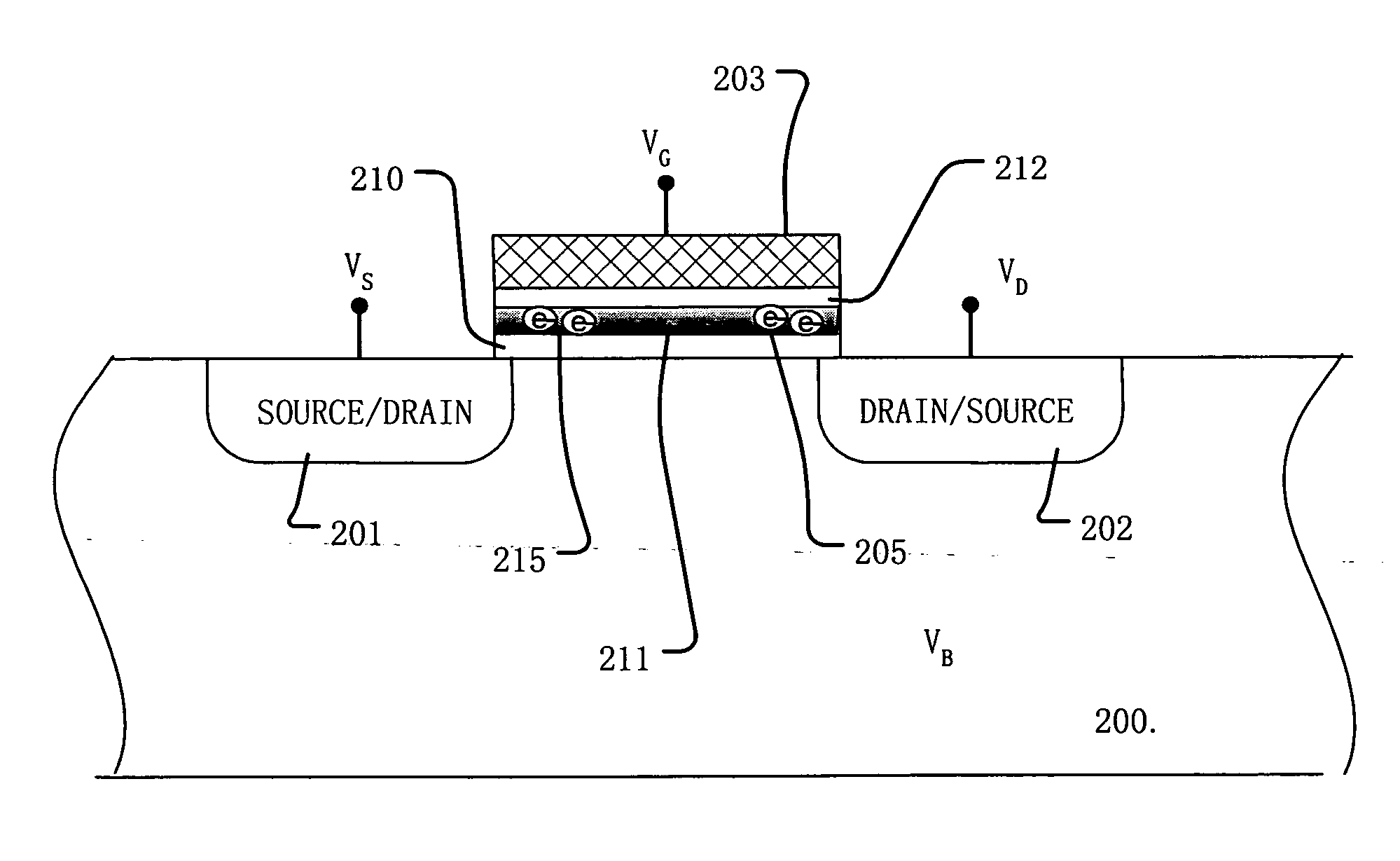
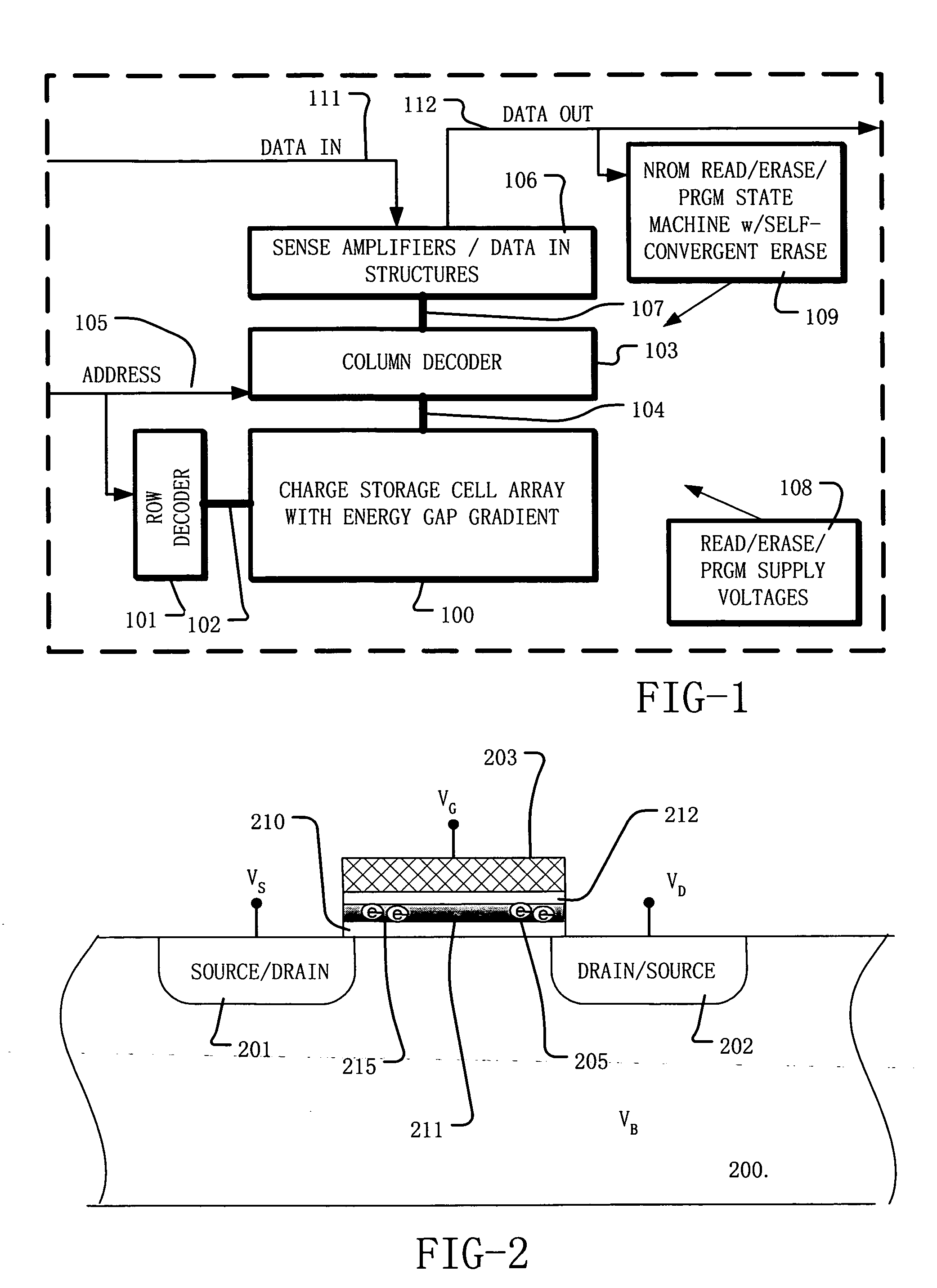
[0022]FIG. 1 is a simplified block diagram of an integrated circuit including charge storage memory cells. The integrated circuit includes a memory array 100 implemented using charge trapping memory cells having a charge trapping dielectric structure with an energy gap gradient. An alternative includes a floating gate memory cell with an interpoly dielectric structure including a middle dielectric layer with an energy gap gradient. The energy gap gradient establishes a weak electric field at equilibrium, opposing charge leakage, and improves charge retention and durability of the memory device. A page / row decoder 101 is coupled to a plurality of word lines 102 arranged along rows in the memory array 100. A column decoder 103 is coupled to a plurality of bit lines 104 arranged along columns in the memory array 100. Addresses are supplied on bus 105 to column decoder 103 ...
PUM
 Abstract
Description
Claims
Application Information
 - R&D
- Intellectual Property
- Life Sciences
- Materials
- Tech Scout
- Unparalleled Data Quality
- Higher Quality Content
- 60% Fewer Hallucinations
Browse by: Latest US Patents, China's latest patents, Technical Efficacy Thesaurus, Application Domain, Technology Topic, Popular Technical Reports.
© 2025 PatSnap. All rights reserved.Legal|Privacy policy|Modern Slavery Act Transparency Statement|Sitemap|About US| Contact US: help@patsnap.com