Reconfigurable logical circuit using transistor having spi-dependent transmission characteristics

Inactive Publication Date: 2006-06-01
JAPAN SCI & TECH CORP
4 Cites 29 Cited by

AI-Extracted Technical Summary

Problems solved by technology

More specifically, the logic blocks that utilizes the LUT method and νMOS have problems in the volatility of logic functions.
Also, problems are caused with respect to the number of devices (the occupied area).
SRAMs are employed for LUTs, the problems are caused by the volatility of the SRAMs.
When the power supply is cut off, the contents of the LUTs, o...

Method used

[0135] In accordance with this embodiment, the operating curve is saturated as in the E/D configuration, and accordingly, the mean logic margin can be made wider. Also, it is effective for low power consumption.
[0180] In the circuit shown in FIG. 30, the number of MOSFETs is 10, and the number of capacitors is 2. As this circuit can be realized with a CMOS configuration, the circuit layout can be made very compact.
[0232] As described so far, any of the logic circuits in accordance with the embodiments of the present inv...

Benefits of technology

[0013] It is therefore an object of the present invention to provide a non-volatilely reconfigurable circuit with a small number of devices. Such a circuit should be small in size and have low power consumption.
[0014] In a circuit in accordance with the present invention, a transistor (hereinafter referred to as “spin transistor”) with transfer characteristics that depend on the spin direction of the conduction carriers or the magnetization states of the ferromagnetic bodies in the transistor is employed, and the input of the transistor is formed with a νMOS transistor. The operating point of the circuit is adjusted to rewrite functions by varying the driving force of the transistor through the control of the magnetization state of the spin transistor. This circuit is based on a novel technique of rewriting functions entirely in terns of hardware, as the characteristics of the device are changed. This circuit differs from a logic block only with a νMOS in that logic functions can be maintained in a n...

Abstract

A nonvolatilely reconfigurable logical circuit is built It is a reconfigurable logical circuit based on the CMOS configuration using the spin MOSFET. By changing the transmission characteristic of each transistor in accordance with the magnetization states of Tr1, Tr2, Tr5, and Tr8 which are spin MOSFETs, it is possible to reconfigure all the two-input symmetric functions AND/OR/XOR/NAND/NOR/XNOR/“1”/“0”. Since it is possible to constitute the logical function by a small number of non-volatile elements, it is possible to reduce the chip area, thereby increasing the speed and reducing the power consumption.

Application Domain

Technology Topic

Image

  • Reconfigurable logical circuit using transistor having spi-dependent transmission characteristics
  • Reconfigurable logical circuit using transistor having spi-dependent transmission characteristics
  • Reconfigurable logical circuit using transistor having spi-dependent transmission characteristics

Examples

  • Experimental program(2)

Example

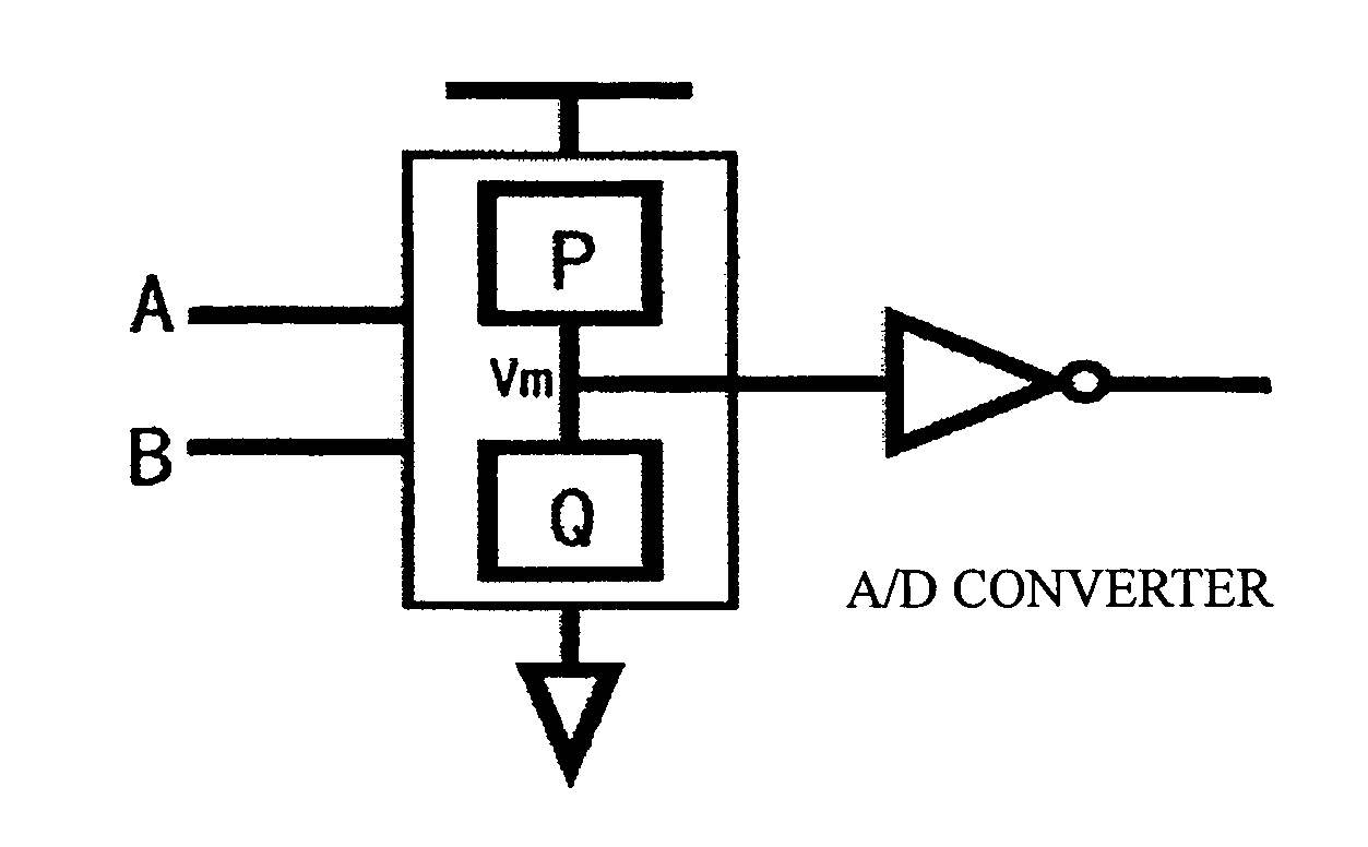
[0122] Next, a reconfigurable logic circuit in accordance with a first embodiment of the present invention is described in conjunction with the accompanying drawings. In the logic circuit in accordance with this embodiment, the driver or the active load of an E/D inverter circuit formed with an enhancement MOSFET and a depletion MOSFET is replaced with a spin MOSFET. To replace the driver, an enhancement spin MOSFET should be employed. To replace the active load, a depletion spin MOSFET should be employed. The input νMOS structure is used for the driver. As for the inverter of the output stage, a CMOS inverter is most preferred in terms of performance, but it is possible to employ an inverter of another type, such as an E/D inverter.
[0123] The load curve in the E/E configuration varies according to the voltage generated in the driver. With the E/D configuration, on the other hand, the load curve with the active load is saturated. Accordingly, a wider logic margin can be allowed.
[0124] 1) AND/OR Circuit
[0125] Referring now to FIGS. 7 through 9, an AND/OR circuit with a n-channel spin MOSFET of a depletion type is described. In FIG. 7, the n-channel spin MOSFET of a depletion type is denoted by Tr1, and the parameter βn1 can be 1 or 10 in the case of antiparallel magnetization or parallel magnetization. Since the source and the gate of Tr1 are short-circuited, the load curve is saturated with respect to Vm as indicated by the solid line in FIG. 8. A νMOS structure is used for the input of a transistor Tr2, and its operation can be as indicated by the broken line in FIG. 8. FIGS. 9A and 9B are the truth tables of this circuit. Also, the details of the operation are shown in Table 1. TABLE 1 Vm A 0 0 1 Vout βn1 B 0 1 1 (in order of Vm) function 1 VO(“1”) VP(“0”) VQ(“0”) “0” “1” “1” OR 10 VO(“1”) VR(“1”) VS(“0”) “0” “0” “1” AND
[0126] In a case where the circuit functions as an OR circuit, the spin MOSFET is put into the antiparalell magnetization configuration, and the parameter βn1 is set at 1, with which the current driving capacity is small. Here, in the case of A=B=“0”, the operating point Vm is V0 according to FIG. 8, and the output Vout is inverted and amplified to “0”. In the case of A or B=“1” (hereinafter, (A, B)=(“1”, “0”) or (A, B)=(“0”, “1”) will be expressed simply as A or B=“1”), the operating point Vm is VP, and accordingly, the output Vout is “1”. In the case of A=B=“1”, the operating point Vm is VQ, and accordingly, the output Vout is “1”.
[0127] In a case where the circuit functions as an AND circuit, the spin MOSFET is put into the paralell magnetization configuration, and the parameter βn1 is set at 10, with which the current driving capacity is large. Here, in the case of A=B=“0”, the operating point Vm is V0, and accordingly, the output Vout is “0”. In the case of A or B=“1”, the operating point Vm is VR, and accordingly, the output Vout is “0”. In the case of A=B=“1”, the operating point Vm is VS, and accordingly, the output Vout is “1”.
[0128] 2) AND/OR/XNOR Circuit
[0129]FIG. 10 illustrates a circuit in which an XNOR function is added to the circuit shown in FIG. 7. The XNOR function is added as a Q group that is a circuit in which the input/output correlation is the same as that in an AND circuit, in the case of A or B=“0” and A=B=“1”, and Vout is “1” (Vm is “0”) in the case of A=B=“0”. In FIG. 10, the transistors Tr3 through Tr5 are the added part. The transistors Tr3 and Tr4 that forms an inverter serve as a level shifter. As shown in FIG. 11, the transistor Tr5 is energized (is put into an ON state) only when A and B are “0”. The transistor Tr5 is a spin MOSFET, but the variation of βn5 according to the magnetization state is designed to be greater than the variation of βn1 of the transistor 1. For example, βn5 is 0.5 or 50 in the case of antiparallel magnetization or parallel magnetization. In the case of parallel magnetization, βn5 is 50, with which a sufficiently high current (Id — high) flows. In the case of antiparallel magnetization, βn5 is 0.5, with which the current value (Id — low) is very small. FIGS. 12A through 14B show the operating point Vm with respect to each parameter β. The sum of currents flowing through the transistors Tr2 and Tr5 is indicated by solid lines, and the current Id — low can be ignored. The circuit functional correlation between βn1 and βn5 is shown in Table 2. TABLE 2 Vm A 0 0 1 Vout βn1 βn5 B 0 1 1 (in order of Vm) function 1 0.5 VO(“1”) VP(“0”) VQ(“0”) “0” “1” “1” OR 10 0.5 VO(“1”) VR(“1”) VS(“0”) “0” “0” “1” AND 1 50 VT(“0”) VR(“1”) VS(“0”) “1” “0” “1” XNOR 10 50 VU(“0”) VR(“0”) VV(“0”) “1” “1” “1” all“1”
[0130] Referring first to FIGS. 12A through 12C, the AND/OR function is described. The transistor Tr5 is put into an antiparalell magnetization configuration, and the current driving capacity is made very small (βn5=0.5). By doing so, the flowing current Id — low can be ignored, and the corresponding portion is regarded as open. As a result, the circuit has the same structure as that of the circuit shown in FIG. 7, and the AND(FIG. 12C)/OR(FIG. 12B) function can be maintained.
[0131] Next, the XNOR function is described in conjunction with FIGS. 13A and 13B. The transistor Tr5 is put into a paralell magnetization configuration, and the current driving capacity is made high (βn5=50). The transistor Tr2 is also put into a paralell magnetization configuration (βn1=10) as in the case of AND. In the case of A=B=“1” or A or B=“1”, the transistor Tr5 is regarded as open, and accordingly, functions as an AND circuit. In the case of A=B=“0”, Vm is discharged by the current Id — high of the transistor Tr5, to obtain Vm=VT inv and Vout=“1”. Further, when the transistor Tr1 is put into an antiparalell magnetization configuration (βn1=1) and the transistor Tr5 is put into a paralell magnetization configuration (βn5=50), Vout becomes “1” for all the inputs (see FIGS. 14A and 14B). This circuit is characterized in that the operating point Vm is always close to 0V or Vdd, and the logic margin is wide.
[0132] 3) AND/OR/XNOR/NAND/NOR/XOR Functions
[0133] In a circuit shown in FIG. 15, another stage of an inverter circuit is added to the output. The details of the operation of this circuit are shown in Table 3. Basically, this circuit is the same as the circuit illustrated in FIG. 10, but all the symmetric Boolean functions can be realized with Vout and its inverted output. TABLE 3 Vout {overscore (Vout)} A 0 0 1 A 0 0 1 βn1 βn5 B 0 1 1 B 0 1 1 function 1 0.5 “0” “1” “1” “1” “0” “0” OR/NOR 10 0.5 “0” “0” “1” “1” “1” “0” AND/NAND 1 50 “1” “0” “1” “0” “1” “0” XNOR/XOR 10 50 “1” “1” “1” “0” “0” “0” all“1”/all“0”

Example

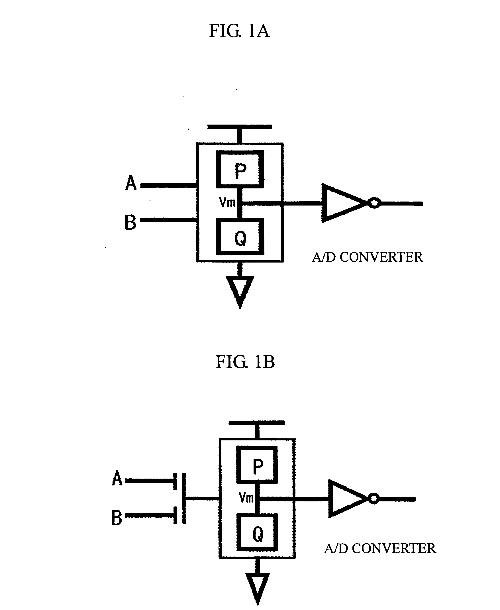
[0134] Next, a reconfigurable logic circuit in accordance with a second embodiment of the present invention is described in conjunction with the accompanying drawings. A logic circuit in accordance with this embodiment can be formed by using a spin MOSFET for either the n-channel MOSFET or the p-channel MOSFET in a CMOS inverter, or using spin MOSFETs for both the n-channel MOSFET and the p-channel MOSFET. The νMOS structure used for the input is formed with a floating gate shared by the n-channel device and the p-channel device. The inverter of the output stage is a conventional inverter of the CMOS configuration.
[0135] In accordance with this embodiment, the operating curve is saturated as in the E/D configuration, and accordingly, the mean logic margin can be made wider. Also, it is effective for low power consumption.
[0136] 1) Threshold Value Variable Inverter
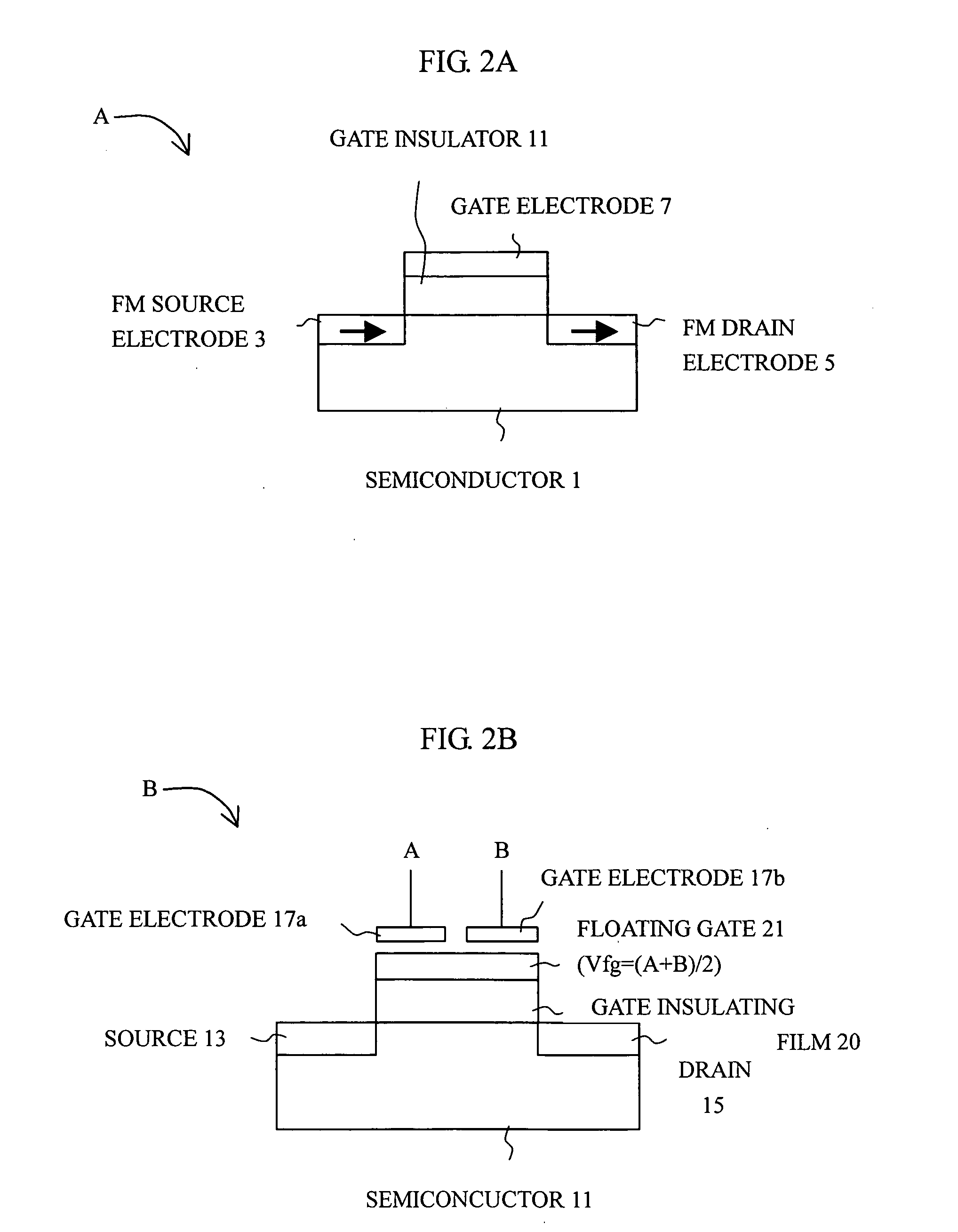
[0137]FIG. 16A is a circuit diagram of an inverter having a variable logic threshold value. In this circuit, the n-channel MOSFET and the p-channel MOSFET of a conventional CMOS inverter are replaced with a p-channel spin MOSFET. Here, the current driving capacity of the p-channel spin MOSFET in the case of parallel magnetization and antiparallel magnetization is made pinv=1 or 10, and the current driving capacity of the n-channel spin MOSFET is a value between 1 and 10. The logic threshold value of the inverter circuit shown in FIG. 16A varies according to the combination of parameters β. FIG. 16B shows the characteristics of both spin MOSFETs in a case where the parameter βninv is fixed while the parameter βpinv is set to 1 or 10. Although the input is constant, the output Vout is VL of the low level when the parameter βpinv is 1, and the output Vout is VH of the high level when the parameter βpinv is 10. In this manner, the output Vout varies according to the current driving capacity of the p-channel spin MOSFET. More quantitatively, this can be explained as follows.
[0138] The inverter circuit shown in FIG. 16A can be considered as the same as a conventional CMOS inverter. In such a case, the p-channel spin MOSFET and the n-channel spin MOSFET operate in the saturation region. With the drain current Id flowing through the n-channel spin MOSFET and the p-channel spin MOSFET, the following equation can be obtained: V inv = V dd - V thp + V thn ⁢ β inv 1 + β inv ⁢ ⁢ where ⁢ ⁢ β inv = β ninv β pinv [ Equation ⁢ ⁢ 1 ]
[0139] Here, the logic threshold value Vinv is plotted as the function of the driving force ratio βinv=βninv/βpinv in FIG. 17, with Vdd being 3.3V and Vthn being |Vthp|=0.5V. As shown in FIG. 17, the threshold value according to the ratio βinv=0.1, 1, 10 can be obtained.
[0140] 2) AND/OR
[0141]FIG. 18 illustrates an AND/OR circuit that employs the threshold value variable inverter shown in FIG. 16A. As shown in FIG. 18, the AND/OR circuit is formed with inverters of two stages. The inverter at the input side is a threshold value variable inverter, and the inverter at the output side is a conventional inverter (with a threshold value Vinv2=Vdd/2). The operating characteristics of the circuit shown in FIG. 18 are shown in FIGS. 19A and 19B. In FIG. 19A, the solid line indicates the characteristics of the transistor Tr1, and the broken line indicates the characteristics of the transistor Tr2. The details of the operation of this circuit are shown in Table 4. TABLE 4 Vm A 0 0 1 Vout βn1 βn2 B 0 1 1 (in order of Vm) function 1 10 VO(“1”) VP(“0”) VQ(“0”) “0” “1” “1 ” OR 10 1 VO(“1”) VR(“1”) VQ(“0”) “0” “0” “1” AND
[0142] 2-1) OR
[0143] Referring now to FIGS. 19A and 19B, an OR circuit is described. In a case where the circuit illustrated in FIG. 18 functions as an OR circuit, the transistor Tr1 is put into an antiparalell magnetization configuration (βp1=1), and the transistor Tr2 is put into a paralell magnetization configuration (βn2=10). Here, in the case of A=B=“0”, the operating point Vm is V0 according to FIG. 19A, and the output Vout is inverted and amplified to “0”. In the case of A or B=“1”, the operating point Vm is VP, and the output Vout is “1”. In the case of A=B=“1”, the operating point Vm is VQ, and the output Vout is “1”.
[0144] 2-2) AND
[0145] Referring now to FIGS. 20A and 20B, an AND circuit is described. The transistor Tr1 is put into a paralell magnetization configuration (βp1=10), and the transistor Tr2 is put into an antiparalell magnetization configuration (βn2=1). Here, in the case of A=B=“0”, the operating point Vm is V0, and the output Vout is inverted and amplified to “0”. In the case of A or B=“1”, the operating point Vm is VR, and the output Vout is “0”. In the case of A=B=“1”, the operating point Vm is VQ, and the output Vout is “1”.
[0146] As can be seen from FIGS. 21 through 23B, the threshold value Vinv1 of the threshold value variable inverter (formed with the transistors Tr1 and Tr2) at the input side may be regarded as the reference value. In the following, the operation in such a case is described.
[0147] 2-3) OR
[0148] When the transistor Tr1 is put into an antiparalell magnetization configuration (βp1=1) and the transistor Tr2 is put into a paralell magnetization configuration (βn2=10) in a circuit illustrated in FIG. 21, the logic threshold value Vinv1 becomes Vinv1 — low dd/2, as shown in FIG. 22A. Also as shown in FIGS. 22A and 22B, in the case of A=B=“0”, Vfg becomes “0”. Accordingly, the operating point Vm is V0=“1”, and the output Vout is “0”. In the case of A or B=“1”, Vfg is Vdd/2>Vinv1 — low, Accordingly, the operating point Vm is VP=“0”, and the output Vout is “1”. In the case of A=B=“1”, Vfg is Vdd. Accordingly, the operating point Vm is VQ=“0”, and the output Vout is “1”.
[0149] 2-4) AND
[0150] When the transistor Tr1 is put into a paralell magnetization configuration (βp1=10) and the transistor Tr2 is put into an antiparalell magnetization configuration (βn2=1) in the circuit illustrated in FIG. 21, the logic threshold value Vinv1 becomes Vinv1 — highVdd/2, as shown in FIG. 23A. In the case of A=B=“0”, Vfg becomes “0”. Accordingly, the operating point Vm is V0=“1”, and the output Vout is “0”. In the case of A or B=“1”, Vfg is Vdd/2 inv1 — low. Accordingly, the operating point Vm is VR=“1”, and the output Vout is “0”. In the case of A=B=“1”, Vfg is Vdd. Accordingly, the operating point Vm is VQ=“0”, and the output Vout is “1”.
[0151] 3) AND/OR/XNOR
[0152]FIG. 24 illustrates an AND/OR/XNOR circuit. The principles of the operation are the same as in the case of the circuit shown in FIG. 10. In the XNOR circuit, the input/output correlation is the same as that in the AND circuit in the case where A=B=“1” or A or B=“1”, but is different from that in the AND circuit only in the case where A=B=“0”, with Vout being “1” (Vm=“0”). This function can be realized by adding a circuit formed with the transistors Tr3, Tr4, and Tr5 (an n-channel spin MOSFET) to the circuit group Q. The inverter (a level shifter) formed with the transistors Tr3 and Tr4 has a threshold value Vinv3 lower than Vdd/2. Accordingly, only in the case where A=B=“0”, Vin — n becomes “1”, and the transistor Tr5 is turned on. The variation in the current driving capacity βn5 of the transistor Tr5 between parallel magnetization and antiparallel magnetization is wider than that in the case of the transistors Tr1 and Tr2, and βn5 is 0.5 (antiparallel magnetization) or 50 (parallel magnetization). In the case of parallel magnetization (βn5=50), a sufficiently high current (Id — high) flows, but in the case of antiparallel magnetization (βn5=0.5), the value of the current (Id — low) is very small (see the upper and lower graphs in FIG. 25).
[0153] The details of the operation are shown in Table 5. TABLE 5 Vm A 0 0 1 Vout (in βp1 βn2 βn5 B 0 1 1 order of Vm) function 1 10 0.5 VO(“1”) VP(“0”) VQ(“0”) “0” “1” “1” OR 10 1 0.5 VO(“1”) VR(“1”) VQ(“0”) “0” “0” “1” AND 1 10 50 VT(“0”) VP(“0”) VQ(“0”) “1” “1” “1” all“1” 10 1 50 VS(“0”) VR(“1”) VQ(“0”) “1” “0” “1” XNOR
[0154] 3-1) AND/OR (See FIGS. 26A and 26B, 27A and 27B)
[0155] As the transistor Tr5 is put into an antiparalell magnetization configuration (βn5=0.5), the current Id — low can be ignored, and the transistor Tr5 can be regarded as open. Accordingly, the circuit becomes equivalent to the AND/OR circuit shown in FIG. 18.
[0156] 3-2) XNOR (See FIGS. 29A and 29B)
[0157] The transistor Tr5 is put into a paralell magnetization configuration (βn5=50). In the inverter part, the transistor Tr1 is put into a paralell magnetization configuration (βp1=10), and the transistor Tr2 is put into an antiparalell magnetization configuration (βn2=1), as in the AND circuit. In the case where A=B=“1” or A or B=“1”, the transistor Tr5 is equivalent to an open circuit, and operates in the same manner as the AND circuit. In the case where A=B=“0”, Vm is discharged by the current Id — high of the transistor Tr5, so as to be Vm=VS inv2. Accordingly, Vout becomes “1”. Where the transistor Tr1 is put into an antiparalell magnetization configuration (βp1=1), the transistor Tr2 is put into a paralell magnetization configuration (βn2=10), and the transistor Tr5 is put into a paralell magnetization configuration (βn5=50), the output Vout becomes “1” for all the input patterns (see FIGS. 28A and 28B).
[0158] Although all symmetric Boolean functions can be realized by adding an inverter to the output of the circuit shown in FIG. 24, a technique of achieving all the symmetric Boolean functions by adding a new circuit to the circuit group P is described below.
[0159] 4) AND/OR/XNOR/XOR
[0160]FIG. 30 illustrates an AND/OR/XNOR/XOR circuit. In the XOR circuit, the input/output correlation is the same as that in the OR circuit in the case where A=B=“1” or A or B=“1”, but is different from that in the OR circuit only in the case where A=B=“1”, with Vout being “0”. Accordingly, this function can be realized by adding a circuit with which Vout becomes “0” in the case where A=B=“1”. The XOR function can be achieved by employing the transistors Tr6, Tr7, and Tr8 (a p-channel spin MOSFET) in a complementary manner together with the transistors Tr3, Tr4, and Tr5 (an n-channel spin MOSFET). The inverter formed with the transistors Tr6 and Tr7 has a threshold value Vinv4 higher than Vdd/2. Accordingly, only in the case where A=B=“1”, Vin — n becomes “0”, and the transistor Tr8 is turned on (see FIG. 31).
[0161] The variation in the current driving capacity βp8 of the transistor Tr8 between parallel magnetization and antiparallel magnetization is wider than that in the case of the transistors Tr1 and Tr2, and βp8 is 0.5 (antiparallel magnetization) or 50 (parallel magnetization). In the case of parallel magnetization (β8p=50), a sufficiently high current (Id — high) flows, but in the case of antiparallel magnetization (βp8=0.5), the value of the current (Id — low) is very small. FIGS. 32A and 32B and FIGS. 33A and 33B show the operating point Vm in the case of the transistor Tr8 is in the paralell magnetization configuration (βp8=50) and the transistor Tr5 is in the antiparalell magnetization configuration (βn5=0.5). The sum of currents flowing through the transistors Tr1 and Tr8 is indicated by solid lines, and the sum of currents flowing through the transistors Tr2 and Tr5 is indicated by broken lines. Here, the current Id — low is ignored.
[0162] The operation of this circuit is shown in Table 6. TABLE 6 Vm A 0 0 1 Vout βn1 βn2 βn5 βp8 B 0 1 1 (in order of Vm) function 1 10 0.5 0.5 “1” “0” “0” “0” “1” “1” OR 10 1 0.5 0.5 “1” “1” “0” “0” “0” “1” AND 1 10 50 0.5 “0” “0” “0” “1” “1” “1” all“1” 10 1 50 0.5 “0” “1” “0” “1” “0” “1” XNOR 1 10 0.5 50 VO(“1”) VP(“0”) VT(“1”) “0” “1” “0” XOR 10 1 0.5 50 VO(“1”) VR(“1”) VT(“1”) “0” “0” “0” all“0”
[0163] 4-1) AND/OR/XNOR
[0164] When the transistor Tr8 is put into an antiparalell magnetization configuration (βp8=0.5) in the circuit shown in FIG. 30, the current flowing through the transistor Tr8 can be ignored, and the transistor Tr8 can be regarded as open. Accordingly, this circuit can be made equivalent to the circuit shown in FIG. 24, and the AND/OR/XNOR functions can be achieved by changing the magnetization states of the transistors Tr1, Tr2, and Tr5 (or the current driving capacities βp1, βn2, and βn5).
[0165] 4-2) XOR (See FIGS. 32A and 32B)
[0166] The transistor Tr8 is put into a paralell magnetization configuration (βp8=50). In the other parts, the transistor Tr1 is put into an antiparalell magnetization configuration (βp1=1), the transistor Tr2 is put into a paralell magnetization configuration (βn2=10), and the transistor Tr5 is put into an antiparalell magnetization configuration (βn5=0.5), as in the OR circuit. In the case where A=B=“0” or A or B=“1”, the transistor Tr8 is open, and operates in the same manner as the OR circuit. In the case where A=B=“1”, Vm is charged with the current Id — high of the transistor Tr8, so as to be Vm=VT inv — 2. Accordingly, Vout becomes “0”. Where the transistor Tr1 is put into a paralell magnetization configuration (βp1=10), the transistor Tr2 is put into an antiparalell magnetization configuration (βn2=1), the transistor Tr5 is put into an antiparalell magnetization configuration (βn5=0.5), and the transistor Tr8 is put into a paralell magnetization configuration (βp8=50), the output Vout becomes “0” for all the input patterns (see FIGS. 33A and 33B).
[0167] 5) AND/OR/XNOR/XOR/NAND/NOR
[0168] As in the case shown in FIG. 15, an inverter may be added to the output of the circuit shown in FIG. 24. However, it is possible to achieve the circuit by employing the circuit shown in FIG. 30. The transistor Tr5 in FIG. 30 functions only in the case where A=B=“0”, and the operating point Vm is “0”. The transistor Tr8 functions only in the case where A=B=“1”, and the operating point Vm is “1”. Taking this fact into consideration, a NAND/NOR can be realized with the circuit shown in FIG. 30.
[0169]FIGS. 33A and 33B and FIGS. 34A and 34B show the operating points in the case where the transistors Tr5 and Tr8 are in a paralell magnetization configuration (βn5=βp8=50) in the circuit shown in FIG. 30. The operations of the circuits are shown in Table 7. TABLE 7 Vm A 0 0 1 Vout βn1 βn2 βn5 βp8 B 0 1 1 (in order of Vm) function 1 10 0.5 0.5 “1” “0” “0” “0” “1” “1” OR 10 1 0.5 0.5 “1” “1” “0” “0” “0” “1” AND 1 10 50 0.5 “0” “0” “0” “1” “1” “1” all“1” 10 1 50 0.5 “0” “1” “0” “1” “0” “1” XNOR 1 10 0.5 50 “1” “0” “1” “0” “1” “0” XOR 10 1 0.5 50 “1” “1” “1” “0” “0” “0” all“0” 1 10 50 50 VT(“0”) VP(“0”) VU(“1”) “1” “1” “0” NAND 10 1 50 50 VS(“0”) VR(“1”) VV(“1”) “1” “0” “0” NOR
[0170] 5-1) AND/OR
[0171] When the transistor Tr5 is put into an antiparalell magnetization configuration (βn5=0.5) and the transistor Tr8 is put into an antiparalell magnetization configuration (βp8=0.5), the transistors Tr5 and Tr8 are both open. Accordingly, this circuit is equivalent to the circuit shown in FIG. 28.
[0172] 5-2) XNOR
[0173] When the transistor Tr5 is put into a paralell magnetization configuration (βn5=50) and the transistor Tr8 is put into an antiparalell magnetization configuration (βp8=0.5), the transistor Tr8 is open. Accordingly, this circuit is equivalent to the circuit shown in FIG. 24.
[0174] 5-3) XOR
[0175] When the transistor Tr5 is put into an antiparalell magnetization configuration (βn5=0.5) and the transistor Tr8 is put into a paralell magnetization configuration (βp8=50), the circuit becomes an XOR equivalent to the circuit shown in FIGS. 32A and 32B.
[0176] 5-4) NAND (See FIGS. 34A and 34B)
[0177] The transistor Tr1 is put into an antiparalell magnetization configuration (βp1=1), the transistor Tr2 is put into a paralell magnetization configuration (βn2=10), the transistor Tr5 is put into a paralell magnetization configuration (βn5=50), and the transistor Tr8 is put into a paralell magnetization configuration (βp8=50). In the case where A=B=“0”, discharging is performed by the transistor Tr5, and the operating point Vm becomes VT inv2. Accordingly, the output Vout becomes “1”. In the case where A or B is “1”, the operating point Vm becomes VP inv2, and accordingly, the output Vout becomes “1”. In the case where A=B=“1”, Vm is charged by the transistor Tr8, so as to be Vm=VUVinv2. Accordingly, Vout becomes “0”.
[0178] 5-5) NOR (See FIGS. 35A and 35B)
[0179] The transistor Tr1 is put into a paralell magnetization configuration (βp1=10), the transistor Tr2 is put into an antiparalell magnetization configuration (βn2=1), the transistor Tr5 is put into a paralell magnetization configuration (βn5=50), and the transistor Tr8 is put into a paralell magnetization configuration (βp8=50). In the case where A=B=“0”, charging is performed by the transistor Tr5, and the operating point Vm becomes VS inv2. Accordingly, the output Vout becomes “1”. In the case where A or B is “1”, the operating point Vm becomes VRVinv2, and accordingly, the output Vout becomes “0”. In the case where A=B=“1”, Vm is charged by the transistor Tr8, so as to be Vm=VVVinv2. Accordingly, Vout becomes “0”.
[0180] In the circuit shown in FIG. 30, the number of MOSFETs is 10, and the number of capacitors is 2. As this circuit can be realized with a CMOS configuration, the circuit layout can be made very compact.
[0181]FIG. 36 shows a circuit in which CMOS inverters using spin MOSFETs are connected in two stages. Each of the first-stage inverter and the second-stage inverter has an input of a νMOS structure. In this circuit, the same weighting is set on inputs A and B. The inputs A and B are input to the second-stage inverter, and the output Vm1 of the first stage is also input to the second-stage inverter. The capacitance weighting is the same between the inputs A and B in the second-stage inverter, but the capacitance weighting differs between the input A (or B) and the output Vm1. For example, with the input capacitance with Vm1 being Cm1, the relationship of 3Cm1=CA (=CB) should be established. In this logic circuit, the magnetization states of Q1, Q2, and Q4 are changed to rewrite the logic functions. With the output Vm1, the logic functions of NOR and NAND can be realized. With the output Vm2, the logic functions of XNOR, XOR, AND, OR, all “1”, and all “0” can be realized. Since the logic amplitude may not reach the “0” level or “1” level with the outputs Vm1 and Vm2, depending on the logic function, it is preferable that a CMOS inverter or the like is added to each output to amplify the signal. In such a case, however, the logic function is inverted. Also, it is possible to employ a spin MOSFET for Q2.
[0182] Next, a logic circuit of a second CMOS configuration is described for reference, in conjunction with the accompanying drawings. In this logic circuit, a threshold value variable inverter is employed as the output-stage inverter, so as to form a rewritable logic circuit. A logic threshold value Vinv is a binary value (Vinv — high or Vinv — low), and is supplied through an inverter that includes a conventional nMOS and a p-channel spin MOSFET. This inverter functions as an A-D converter that amplifies an analog voltage (“½” as described below) to a digital logic level (“0” or “1”), but also controls the threshold value. The output-stage A-D converter can be realized by employed the logic threshold value variable inverter, with the spin MOSFETs of the E/E, E/D, and CMOS inverters (shown in FIG. 6) having the νMOS structure for the inputs being replaced with conventional MOSFETs. In the following, other circuits are described for reference.
[0183] 1) NAND/NOR
[0184]FIG. 37 illustrates an example structure of a NAND/NOR circuit. This circuit differs from the circuit illustrated in FIG. 48, in that the value of Vm is not varied by spin MOSFETs but the threshold value is varied when the threshold value is amplified to the logic level by the inverter. As shown in FIG. 38, the load curve (the characteristics of the νMOS structure) of the logic circuit shown in FIG. 37 is represented by a single line, and the operating points are indicated only by VO, VP, and VQ. Here, the functions are changed by varying the operating point with the logic threshold value Vinv that is higher (Vinv — high) or lower (Vinv — low) than the operating point VP when A or B is “1”. The region between the values Vinv — high and Vinv — low is “½”. FIG. 39 shows the truth table in this case, and Table 8 shows the details of the operation of the above circuit. TABLE 8 Vm A 0 0 1 Vout (in Vinv B 0 1 1 order of Vm) function Vinv_low VO(“0”) VP(“½”) VQ(“1”) “1” “0” “0” NOR Vinv_high VO(“0”) VP(“½”) VQ(“1”) “1” “1” “0” NAND
[0185] In the case where A=B=“0”, the operating point Vm is VO inv — low, Vinv — high, and the output Vout becomes “1” with the inverter. In the case where A=B=“1”, the operating point Vm is VQ inv — low, Vinv — high, and the output Vout becomes “0” with the inverter. Here, the outputs do not depend on the logic threshold value Vinv of the inverter. In the case where A or B is “1”, the relationship Vinv — low P inv — high is established. In this case, if the threshold value Vinv is equal to Vinv — low, the output Vout is “0”, and accordingly, the circuit functions as a NOR circuit. If the threshold value Vinv is equal to Vinv — high, the output Vout is “1”, and accordingly, the circuit functions as a NAND circuit.
[0186] 2) NAND/NOR/XOR
[0187]FIG. 40 illustrates a NAND/NOR+XNOR circuit. FIG. 41 shows the operating points of the circuit. The principles of the operation of this circuit are the same as those shown in FIGS. 50 through 54. In NOR, the circuit that has the output Vout=“1” (Vm=“0”, accordingly) in the case where A=B=“1” is formed with the transistors Tr3, Tr4, and Tr5 (an n-channel spin MOSFET). The transistor Tr5 is either in a high driving force state (βn5=10) or in a low driving force state (βn5=1). The details of the operation are shown in Table 9. TABLE 9 Vm A 0 0 1 Vout Vinv βn5 B 0 1 1 (in order of Vm) function Vinv_low 1 VO(“0”) VP(“½”) VQ(“1”) “1” “0” “0” NOR Vinv_high 1 VO(“0”) VP(“½”) VQ(“1”) “1” “1” “0” NAND Vinv_low 10 VO(“0”) VP(“½”) VR(“0”) “1” “0” “1” XNOR Vinv_high 10 VO(“0”) VP(“½”) VR(“0”) “1” “1” “1” all“1”
[0188] 2-1) NAND/NOR (SeeFIGS. 42A and 42B)
[0189] In the circuit shown in FIG. 40, the transistor Tr5 is put into the state in which βn5 is “1”, so that the drain current Iid — low can be ignored. Accordingly, the transistor Tr5 can be regarded as open, and the circuit becomes equivalent to the NAND/NOR circuit shown in FIG. 37.
[0190] 2-2) XNOR (See FIGS. 43A and 43B)
[0191] In FIG. 45, the transistor Tr5 is put into the state in which βn5 is 10, and the threshold value of the inverter is set at Vinv — low as in the NOR circuit. In the case where A=B=“0” or A or B=“1”, the transistor Tr5 is regarded as open, and operates in the same manner as the NOR circuit. In the case where A=B=“1”, Vm is charged with the current Id — high of the transistor Tr5, so as to be Vm=VR inv — low, and the output Vout becomes “1”.
[0192] Further, when the transistor Tr5 is put into the state in which βn5 is 10 and the threshold value is set at Vinv — high, the output Vout becomes “1” for all inputs.
[0193] 3) NAND/NOR/XNOR/XOR
[0194]FIG. 44 illustrates a NAND/NOR/XNOR/XOR circuit. In the XOR circuit, the input/output correlation is the same as that in the NAND circuit in the case where A=B=“1” or A or B=“1”, but is different from that in the AND circuit only in the case where A=B=“0”, with Vout being “0”. Accordingly, this function can be realized by adding a circuit with which Vout becomes “0” (with Vm being “1”) in the case where A=B=“0”. The XOR function can be achieved by employing the p-channel transistors Tr6, Tr7, and Tr8 (a p-channel spin MOSFET) in a complementary manner together with the n-channel transistors Tr3, Tr4, and Tr5 (an n-channel spin MOSFET). The transistor Tr8 is either in a high driving force state (βp8=10) or a low driving force state (βp8=1). The source follower of the transistors Tr6 and Tr7 is a positive level shifter, and the transistor Tr8 is turned on only in the case where A=B=“0”.
[0195]FIG. 45 shows the operating characteristics of the transistors Tr6 and Tr7. According to the operating characteristics, Vin — p is determined. The operating point VD in the case where A=B=“1” and the operating point VE in the case where A or B is “1” are both higher than the threshold value of the transistor Tr8. Accordingly, no current flows, and the circuit can be regarded as open. Only with the operating point VF in the case where A=B=“0”, the transistor Tr8 is turned on. (If p-channel spin MOSFETs with threshold values higher than Vdd/2 can be integrated, the transistors Tr6 and Tr7 are unnecessary, and the Vfg node should be connected directly to the gate of the transistor Tr8.) In the case where βp8 is 10, a sufficiently high current Id — high flows, but in the case where βp8 is 1, the value of the current (Id — low) is very small. FIGS. 46A and 46B show the operating points Vm in the case where βp8 is 10 and in the case where βn5 is 1. The sum of the currents flowing through the transistors Tr1 and Tr8 is indicated by solid lines, and the current Id — low is ignored in FIGS. 46A and 46B.
[0196] The details of the operation are shown in Table 10. TABLE 10 Vm A 0 0 1 Vout Vinv βn5 βp8 B 0 1 1 (in order of Vm) function Vinv_low 1 1 “0” “½” “1” “1” “0” “0” NOR Vinv_high 1 1 “0” “½” “1” “1” “1” “0” NAND Vinv_low 10 1 “0” “½” “0” “1” “0” “1” XNOR Vinv_high 10 1 “0” “½” “0” “1” “1” “1” all“1” Vinv_low 1 10 VO(“1”) VP(“½”) VQ(“1”) “0” “0” “0” all“0” Vinv_high 1 10 VO(“1”) VP(“½”) VQ(“1”) “0” “1” “0” XOR
[0197] 3-1) NAND/NOR/XNOR
[0198] The transistor Tr8 is put into a non-driving force state (βp8=1), so that the current flowing through the transistor Tr8 can be ignored. Accordingly, this part can be regarded as open, and the circuit becomes equivalent to the circuit shown in FIG. 40. By simply changing βn5 and Vinv, the NAND/NOR/XOR functions can be maintained.
[0199] 3-2) XOR
[0200] The transistor Tr8 is put into the state in which βp8 is 10, and the threshold value of the inverter is set at Vinv — high as in the NAND circuit. The transistor Tr5 is put into the state in which βn5 is 1, so as to be open. In the case where A=B=“1” or A or B=“1”, the transistor Tr8 is open, and operates in the same manner as the NAND circuit. In the case where A=B=“0”, Vm is charged by the p-channel spin MOSFET, so as to be Vm=VO inv — high, and the output Vout becomes “0”. Further, when the transistor Tr8 is put into the state in which βp8 is 10 and the threshold value is set at Vinv — low, the output Vout becomes “0” for all inputs.
[0201] 4) NAND/NOR/XNOR/XOR/OR/AND
[0202] In the circuit shown in FIG. 44, the transistor Tr5 functions only in the case where A=B=“1”, and Vm is “0”. The transistor Tr8 functions only in the case where A=B=“0”, and Vm is “1”.
[0203] Taking this fact into consideration, an OR/AND can be realized with the circuit shown in FIG. 44. In the circuit, the number of MOSFETs is 10, and the number of capacitors is 2. FIG. 40A shows the load curve in the case where βn5=βp8=10 in FIG. 44. Although the spin MOSFETs of two different types having different rates of change in driving force (the rate of change between Tr1 and Tr2 is 10, and the rate of change between Tr5 and Tr8 is 100, for example) need to be integrated in the circuit shown in FIG. 30, the circuit shown in FIG. 44 requires only one type of spin MOSFET.
[0204] The details of the operation are shown in Table 11. TABLE 11 Vm A 0 0 1 Vout Vinv βn5 βp8 B 0 1 1 (in order of Vm) function Vinv_low 1 1 “0” “½” “1” “1” “0” “0” NOR Vinv_high 1 1 “0” “½” “1” “1” “1” “0” NAND Vinv_low 10 1 “0” “½” “0” “1” “0” “1” XNOR Vinv_high 10 1 “0” “½” “0” “1” “1” “1” all“1” Vinv_low 1 10 “1” “½” “1” “0” “0” “0” all“0” Vinv_high 1 10 “1” “½” “1” “0” “1” “0” XOR Vinv_low 10 10 VO(“1”) VP(“½”) VR(“0”) “0” “0” “1” AND Vinv_high 10 10 VO(“1”) VP(“½”) VR(“0”) “0” “1” “1” OR
[0205] 4-1) NAND/NOR (See FIGS. 46A and 46B)
[0206] With βn5 being 1 and βp8 being 1, the transistors Tr5 and Tr8 are both open. Accordingly, this circuit is equivalent to the circuit shown in FIG. 37, and functions as a NOR ciruict with Vinv — low, and as a NAND circuit with Vinv — high.
[0207] 4-2) XNOR
[0208] With βn5 being 10 and βp8 being 1, the transistor Tr8 is open with Vinv — low. Accordingly, this circuit is equivalent to the circuit shown in FIG. 43, and functions as a XNOR circuit.
[0209] 4-3) XOR
[0210] With βn5 being 1 and βp8 being 10, this circuit is equivalent to the circuit shown in FIG. 9B, and functions as a XNOR circuit.
[0211] 4-4) AND/OR
[0212] The value βn5 is set at 10, and the value βp8 is set at 10 in the circuit shown in FIG. 44 (see FIGS. 47A and 47B). In the case where A=B=“0”, charging is performed by the transistor Tr8, and the operating point V=VOVinv — low, Vinv — high. Accordingly, the output Vout becomes “0”. In the case where A=B=“1”, discharging is performed by the transistor Tr5, and the operating point Vm becomes VQ inv?low, Vinv — high. Accordingly, the output Vout becomes “1”. In the case where A or B is “1”, the transistors Tr5 and Tr8 are both open, and accordingly, the circuit becomes equivalent to the circuit shown in FIG. 37. Since the relationship Vinv — low P inv — high is established, the circuit functions as an AND circuit, with Vinv being Vinv?low. The circuit functions as an OR circuit, with Vinv being Vinv — high.
[0213] The above circuit may be of either an n-channel type or a p-channel type, as long as the transistors Tr1 and Tr2 are of the same conductivity type in each circuit diagram.
[0214] In the following, a logic circuit in accordance with the above examples of reconfigurable circuits using spin MOSFETs is described in conjunction with the accompanying drawings. This logic circuit employs circuit groups including enhancement MOSFETs and n-channel spin MOSFETs.
[0215] 1) NAND/NOR Circuit
[0216]FIG. 48 illustrates an example structure of a rewritable NAND/NOR circuit. As shown in FIG. 48, a rewritable NAND/NOR circuit includes a logic gate stage and an inverter stage. The logic gate stage has a series-connection structure in which a νMOS (Tr1) and a spin MOSFET (Tr2) are connected in series. The νMOS (Tr1) has two inputs A and B, and the voltage Vfg to be applied to the floating gate according to the input value is determined by the equation: (A+B)/2, for example. The current gain of the νMOS (Tr1) is represented by βn1. The inputs are represented by A and B, and the output is represented by Vout, which is either “0” (Low level, 0V) or “1” (High level, the source voltage Vdd). The above νMOS (Tr1) functions as a D-A converter that converts a digital input of “0” or “1” to a voltage of 0, Vdd/2, or Vdd.
[0217] Tr2 is a spin MOSFET (distinguished from a conventional MOSFET by the addition of an arrow), and a constant bias Vb is applied to Tr2. The driving force can be either βn2=1 or βn2=10, depending on the magnetization state stored in the spin MOSFET (Tr2).
[0218] The static characteristics of the spin MOSFET (Tr2) are shown by the solid line in FIG. 6. The νMOS (Tr1) and the spin MOSFET (Tr2) function as a source follower circuit. The νMOS (Tr1) charges the Vm node, which is the connecting point between the νMOS (Tr1) and the spin MOSFET (Tr2), with the driving force according to Vfg. The spin MOSFET (Tr2) discharges the Vm node with the driving force according to the magnetization state. The νMOS (Tr1) and the spin MOSFET (Tr2) constitute the logic gate. FIG. 49 shows the load curve according to the νMOS (Tr1) (indicated by the broken line) and the operating points (VO through VS) of this logic gate.
[0219] The analog voltage Vm supplied at the operating points (VO through VS) is inverted and amplified to the digital logic level “0” or “1” by an inverter with the characteristics shown in the lower half of FIG. 49, with Vinv being the threshold value. The analog voltage Vm is then output to an output terminal Vout.
[0220] Table 12 shows the relationship among βn2, the operating points, and the circuit functions. TABLE 12 Vm A 0 0 1 Vout βn2 B 0 1 1 (in order of Vm) function 1 VO(“0”) VS(“1”) VQ(“1”) “1” “0” “0” NOR 10 VO(“0”) VR(“0”) VP(“1”) “1” “1” “0” NAND
[0221] The driving force of the spin MOSFET (Tr2) in a paralell magnetization configuration is βn2=10. In the case where A=B=“0”, the drain current Id is 0. The analog voltage Vm is VO inv, and the output Vout is “1”, with the inverting amplification of the A-D converter being taken into consideration. In the case where A=B=“1”, the drain current Id is expressed as Id=βn1(Vdd−Vm−Vth)2/2. Here, Vm is VPVinv, and Vout is “0”. The above outputs do not depend on the driving force βn2 of the spin MOSFET (Tr2) (not depending on whether the magnetization state is parallel or antiparallel). In the case where A or B is “1”, the drain current Id is expressed as Id=βn1 (Vdd/2−Vm−Vth)2. Here, one of the inputs is “1”, and Vm is discharged by Tr2. As a result, Vm becomes VR inv, and Vout is “1”. Thus, the circuit functions as a NAND circuit.
[0222] The driving force of the spin MOSFET (Tr2) in an antiparalell magnetization configuration is βn2=1. In the case where A=B=“0”, the analog voltage Vm is VO inv, and the output Vout is “1”, with the inverting amplification of the A-D converter being taken into consideration. In the case where A=B=“1”, Vm is VQVinv, and Vout is “0”. The above outputs do not depend on the driving force βn2 of the spin MOSFET (Tr2) (not depending on whether the magnetization state is parallel or antiparallel). In the case where A or B is “1”, Vm is charged by Tr1. As a result, Vm becomes VSVinv, and Vout is “0”. Thus, the circuit functions as a NOR circuit. FIG. 50 shows the truth table of the circuit shown in FIG. 48.
[0223] As shown in Table 12, based on whether the driving force βn2, which can vary according to the magnetization state in the spin MOSFET, is 1 or 10, a NOR logic or a NAND logic can be selected as the output Vout in response to the inputs A and B. Since the magnetization state of the spin MOSFET is stored in a non-volatile manner, a NOR logic or a NAND logic can be selected in a single circuit. If a circuit having such a function is formed with a conventional CMOS digital circuit, ten MOSFETs are necessary. The circuit of this example is advantageous in that the same function can be realized with only four MOSFETs.
[0224] 2) NAND/NOR+XNOR
[0225] Referring now to FIG. 51A, a rewritable NAND/NOR+XNOR circuit is described. In an XNOR circuit, the input/output correlation is the same as that in an NOR circuit, in the case of A=B=“0” or A or B=“1”. The input/output correlation is different from that in an NOR circuit only in the case where A=B=“1”, with Vout being “1”. Therefore, in the case where A=B=“1”, Vout should be set to “1” (Vm being “0”). Here, a circuit that is formed with two conventional nMOSFETs (Tr3 and Tr4) and one n-channel spin MOSFET (Tr5) is added. The n-channel spin MOSFET (Tr5) can be switched between a high driving force state (βn5=10) and a low driving force state (βn5=1) in accordance with the magnetization state.
[0226] The source followers of Tr3 and Tr4 form a negative level shifter, and Tr5 is turned on only in the case where A=B=“1”. In FIG. 51B illustrating the operation, the upper graph shows the operating characteristics of Tr3 and Tr4 in FIG. 8. According to the operating characteristics, Vin — n is determined. The static characteristics of Tr4 are indicated by the solid line, and the load curve of Tr3 is indicated by the broken lines. The operating point VC in the case where A=B=“0” and the operating point VD in the case where A or B is “1” are smaller than the threshold value of Tr5. Therefore, no current flows in Tr5, which can be regarded as open. Only the gate voltage of Tr5 at the operating point VE in the case where A=B=“1” is greater than the threshold. Accordingly, Tr5 is turned on. If n-channel spin MOSFETs with threshold values greater than Vdd/2 can be integrated, Tr3 and Tr4 are not necessary, and the Vfg node should be connected directly to the gate of Tr5. In the case where βn5 is 10, a sufficiently high current Id — high flows, but in the case where βn5 is 1, the value of the current (Id — low) is very small, as can be seen from the lower graph in FIG. 8B.
[0227]FIGS. 52A through 54B show the operating points Vm with the respective values of β. The sum of the currents flowing through Tr2 and Tr5 is indicated by the solid lines, and the current Id — low is ignored. Table 13 collectively shows the relationship between βn2, βn5, and the functions of the circuit. TABLE 13 Vm A 0 0 1 Vout βn2 βn5 B 0 1 1 (in order of Vm) function 1 1 VO(“0”) VS(“1”) VQ(“1”) “1” “0” “0” NOR 10 1 VO(“0”) VR(“0”) VP(“1”) “1” “1” “0” NAND 1 10 VO(“0”) VS(“1”) VU(“0”) “1” “0” “1” XNOR 10 10 VO(“0”) VR(“0”) VV(“0”) “1” “1” “1” all“1”
[0228]FIGS. 52A and 52B illustrate the NAND/NOR functions. Tr5 is put into a non-driving force state (βn5=1), so that the current flowing through Tr5 can be ignored. Accordingly, the part of Tr5 (FIG. 51A) can be regarded as open. Thus, the NAND/NOR functions can be maintained.
[0229]FIGS. 53A and 53B illustrate the XNOR function. Tr5 is put into a high driving force state (βn5=10), and Tr2 is put into the state in which βn2=1. In the case where A=B=“0” or A or B=“1”, Tr5 is regarded as open, and operates in the same manner as the NOR circuit. In the case where A=B=“1”, Vm is discharged with the current Vinv — high of Tr5, so as to be Vm=VU inv, and the output Vout becomes “1”. Further, when Tr5 is put into the state in which βn5 is 10 and Tr2 is put into the state in which βn2 is 10, the output Vout becomes “1” for all inputs (all “1”), as shown in FIGS. 11A and 11B.
[0230] 3) NAND/NOR/XNOR+AND/OR/XOR Functions
[0231] Another stage of inverter is added to the output terminal Vout shown in FIG. 51A, so that Vout is inverted. As shown in FIG. 55, NAND/NOR/XNOR becomes AND/OR/XOR. With the two outputs of Vout and the inverted Vout, a circuit that can achieve all the symmetric Boolean functions of NAND/NOR/XNOR+AND/OR/XOR, all “0”, and “1” can be formed. In the entire circuit, nine MOSFETs and two capacitances are required. If necessary, a circuit (a pass transistor) for selecting either Vout or the inverted Vout is added to the output terminal, thereby restricting the number of outputs to 1. Table 14 collectively shows the functions of the circuit illustrated in FIG. 55. TABLE 14 Vout {overscore (Vout A 0 0 1 A 0 0 1 βn2 βn5 B 0 1 1 B 0 1 1 function 1 1 “1” “0” “0” “0” “1” “1” NOR/OR 10 1 “1” “1” “0” “0” “0” “1” NAND/AND 1 10 “1” “0” “1” “0” “1” “0” XNOR/XOR 10 10 “1” “1” “1” “0” “0” “0” all“1”/all“0”
[0232] As described so far, any of the logic circuits in accordance with the embodiments of the present invention includes a spin transistor or a spin MOSFET that can change the current driving force in a non-volatile manner, and a νMOS structure. In such a structure, symmetric Boolean functions that are reconfigurable in a non-volatile manner can be realized with a small number of devices. With this circuit, the chip area can be reduced, and high-speed, low-consumption electric operations can be expected. Accordingly, this circuit can be applied to the integrated circuits for mobile devices that are produced in a short time.
[0233] Although the logic circuits in accordance with the specific examples and embodiments of the present invention have been described so far, the present invention is not limited to them. It should be obvious to those skilled in the art that various changes and modifications can be made to the above examples and embodiments, and various combinations of them can also be made.
INDUSTRIAL APPLICABILITY
[0234] Using a logic circuit of the present invention, symmetric Boolean functions that are reconfigurable in a non-volatile manner can be realized with a smaller number of devices. Since a circuit of the present invention can maintain each logic function in a non-volatile manner, there is no need to employ a non-volatile memory for storing logic functions. Accordingly, the chip size can be reduced. Also, using a circuit with a smaller number of devices, high-speed, low-consumption electric operations can be expected. Thus, the circuits of the present invention can be applied to the integrated circuits for mobile devices that are produced in a short time.

PUM

no PUM

Description & Claims & Application Information

We can also present the details of the Description, Claims and Application information to help users get a comprehensive understanding of the technical details of the patent, such as background art, summary of invention, brief description of drawings, description of embodiments, and other original content. On the other hand, users can also determine the specific scope of protection of the technology through the list of claims; as well as understand the changes in the life cycle of the technology with the presentation of the patent timeline. Login to view more.

Similar technology patents

Medical manipulator

Owner:KARL STORZ GMBH & CO KG

Classification and recommendation of technical efficacy words

  • Low power consumption
  • Small size

Rectenna

Owner:IHI AEROSPACE CO LTD
Why Eureka
Try Eureka