One time programmable latch and method

a latch and one-time technology, applied in the field of latch circuits, can solve the problems of exacerbated drawbacks, lost storage data value of volatile storage elements, and area needed to implement such circuits, and achieve the effect of a compact circui

Active Publication Date: 2006-06-01
INFINEON TECH LLC
View PDF29 Cites 10 Cited by
  • Summary
  • Abstract
  • Description
  • Claims
  • Application Information

AI Technical Summary

Benefits of technology

[0020] In such an arrangement, a programmable latch can include but one OTP device to store a value in a nonvolatile fashion, and load such value into a store circuit, such as latch. This can result in an advantageously compact circuit as compared to approaches that utilize two OTP devices.
[0021] ...

Problems solved by technology

Conversely, a volatile storage element will lose a stored data value once power is removed.
A drawback to the above conventional arrangements can be the area needed to implement such circuits.
The above drawbacks are exacerbate...

Method used


Image

  • One time programmable latch and method
  • One time programmable latch and method
  • One time programmable latch and method

Examples


first embodiment

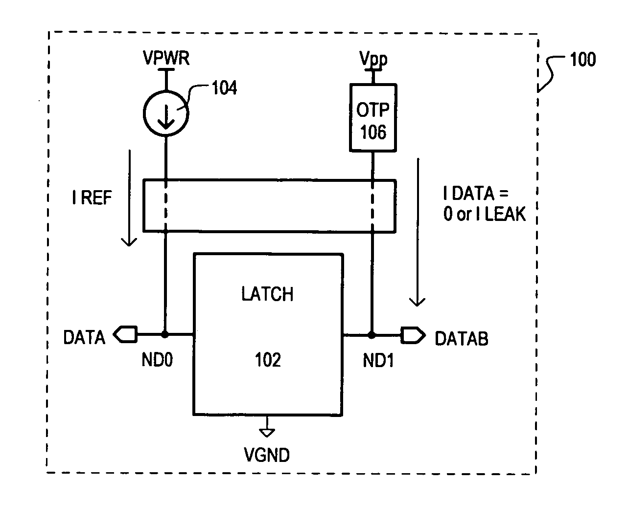
[0064] Referring now to FIG. 1, a programmable latch circuit is set forth in a block schematic diagram and designated by the general reference character 100. The programmable latch circuit can be a one-time programmable (OTP) latch circuit, and can include a latch section 102, a current source circuit 104, and an OTP circuit 106. A latch circuit 102 can be a volatile storage circuit that can latch a data value DATA. For example, a latch circuit 102 can provide complementary data values DATA and DATAB on complementary data nodes ND0 and ND1.

[0065] A current source circuit 104 can provide a reference current IREF to latch circuit 102. In one embodiment, the magnitude of a reference current IREF can be greater than a current drawn by an OTP circuit 106 when storing one state, but less than a current drawn by an OTP circuit 106 when storing a second state. A current source circuit 104 does not utilize any nonvolatile device to generate the reference circuit.

[0066] An OTP circuit 106 c...

second embodiment

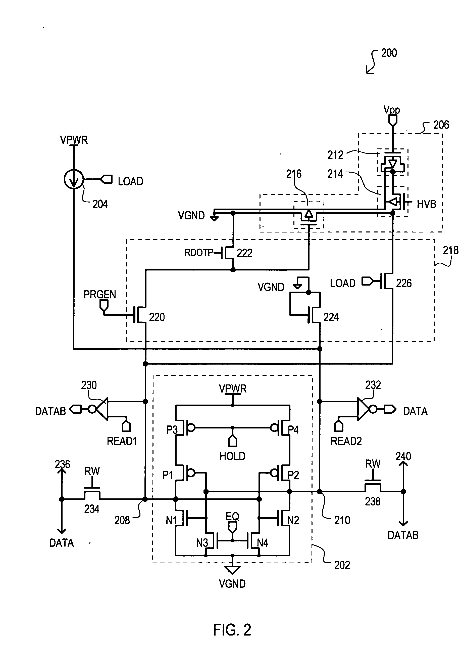
[0069] A one-time programmable (OTP) latch circuit is set forth in FIG. 2, and designated by the general reference character 200. An OTP latch circuit 200 can be considered related to that of FIG. 1, in that FIG. 2 can represent a particular implementation of general circuit set forth in FIG. 1. An OTP latch circuit 200 can include a latch section 202, a current reference circuit 204, an OTP circuit 206, and a load / program circuit 218.

[0070] A latch section 202 can include n-channel insulated gate field effect transistors (NFET(NMOS)s) N1 and N2 cross-coupled between data nodes 208 and 210. Similarly, p-channel insulated gate field effect transistors (PFETs) P1 and P2 can be cross-coupled between data nodes 208 and 210. Looked at in another way, latch circuit 202 can include cross-coupled inverters N1 / P1 and N2 / P2.

[0071] A latch circuit 202 can further include “hold” PFETs P3 and P4. Hold PFET P3 can have a source-drain path coupled between data node 208 and a high supply voltage ...


PUM


Abstract

A one-time programmable (OTP) latch circuit can include a single OTP device capable of storing a logic value in a nonvolatile fashion, or only two OTP devices in the event redundancy is desired. A latch section can latch a data value based on a comparison between a current drawn according to the one OTP device, and a reference current generated without and OTP device. An OTP device can include a gate oxide antifuse (GOAF) device.

Description

[0001] This application claims the benefit of U.S. Provisional Patent Application Ser. No. 60 / 613,179, filed on Sep. 24, 2004.TECHNICAL FIELD [0002] The present invention relates generally to latch circuits and more particularly to latch circuits that can operate in conjunction with nonvolatile storage elements. BACKGROUND OF THE INVENTION [0003] Electronic systems can typically include a data storage capability. For example, bi-stable circuits, such as flip-flops can maintain a data value in one of two binary logic values depending upon an input to the flip-flop. One commonly used bi-stable circuit that can maintain a logic value until another value is written or rewritten is a latch. [0004] A latch can take a number of different forms. For example, a latch can include cross-coupled inverters that can latch a data value on complementary data nodes until a new data value is rewritten. Such latches are often used as static random access memory (SRAM) cells. An SRAM type latch can sto...

Claims


Application Information

Patent Timeline
IPC IPC(8): H03K19/173
CPCG11C14/00G11C17/146G11C17/16G11C16/06G11C16/10G11C16/30
Inventor TAHERI, BABAKMAHESHWARI, SANJEEV
Owner INFINEON TECH LLC
Why Eureka
Try Eureka