
Semiconductor integrated circuit designing method and program

a technology of integrated circuits and integrated circuits, applied in the direction of cad circuit design, program control, instruments, etc., can solve the problems of inability to improve the yield of loose design rules, the inability to shorten the inability to solve the inability to reduce the number of wirings derived from replacement with a first cell, so as to reduce the time required for automatic arrangement and connection, the effect of preventing the inability to reduce the number of wiring

Inactive Publication Date: 2006-06-01
SOCIONEXT INC
View PDF13 Cites 9 Cited by
  • Summary
  • Abstract
  • Description
  • Claims
  • Application Information

AI Technical Summary

Benefits of technology

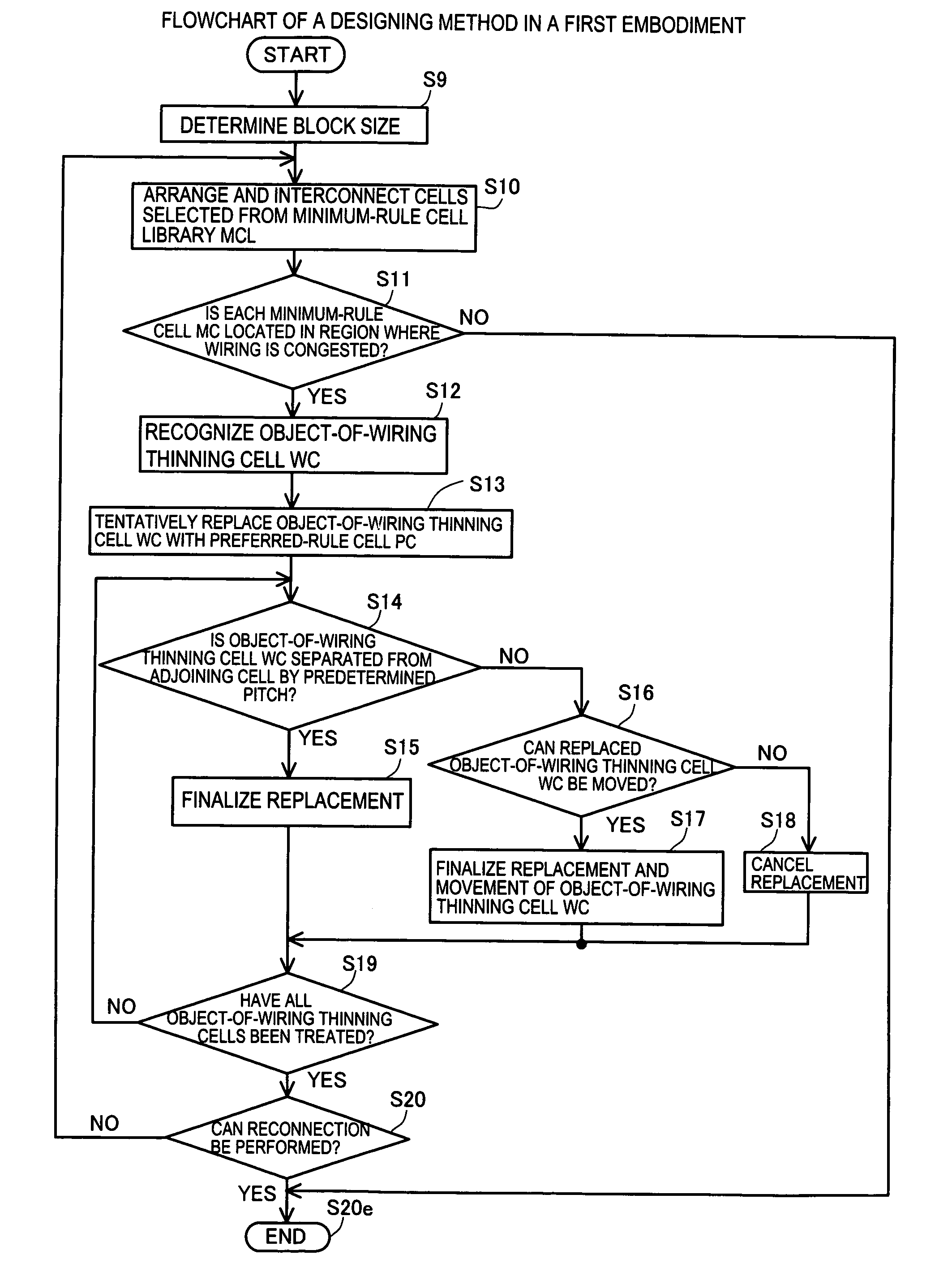
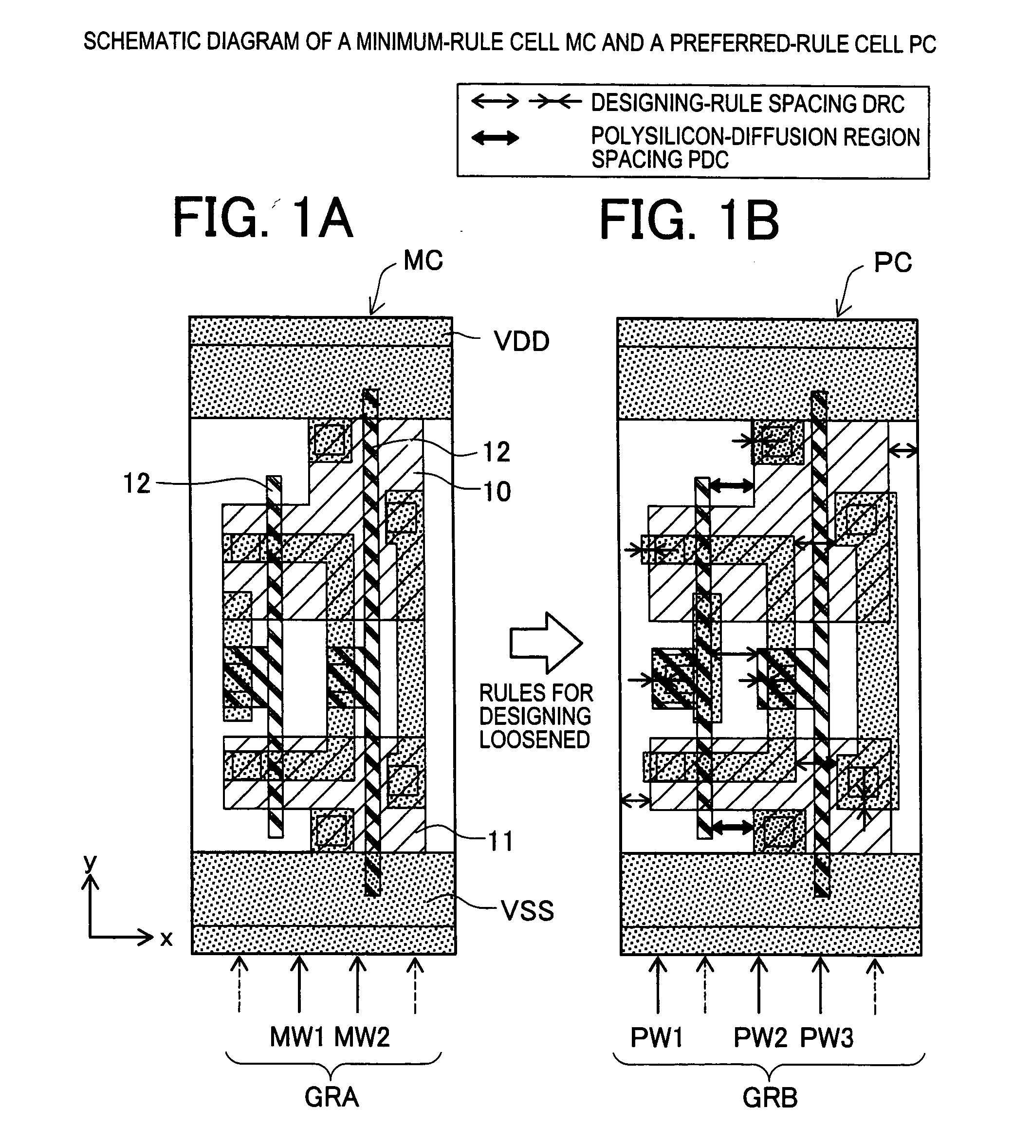
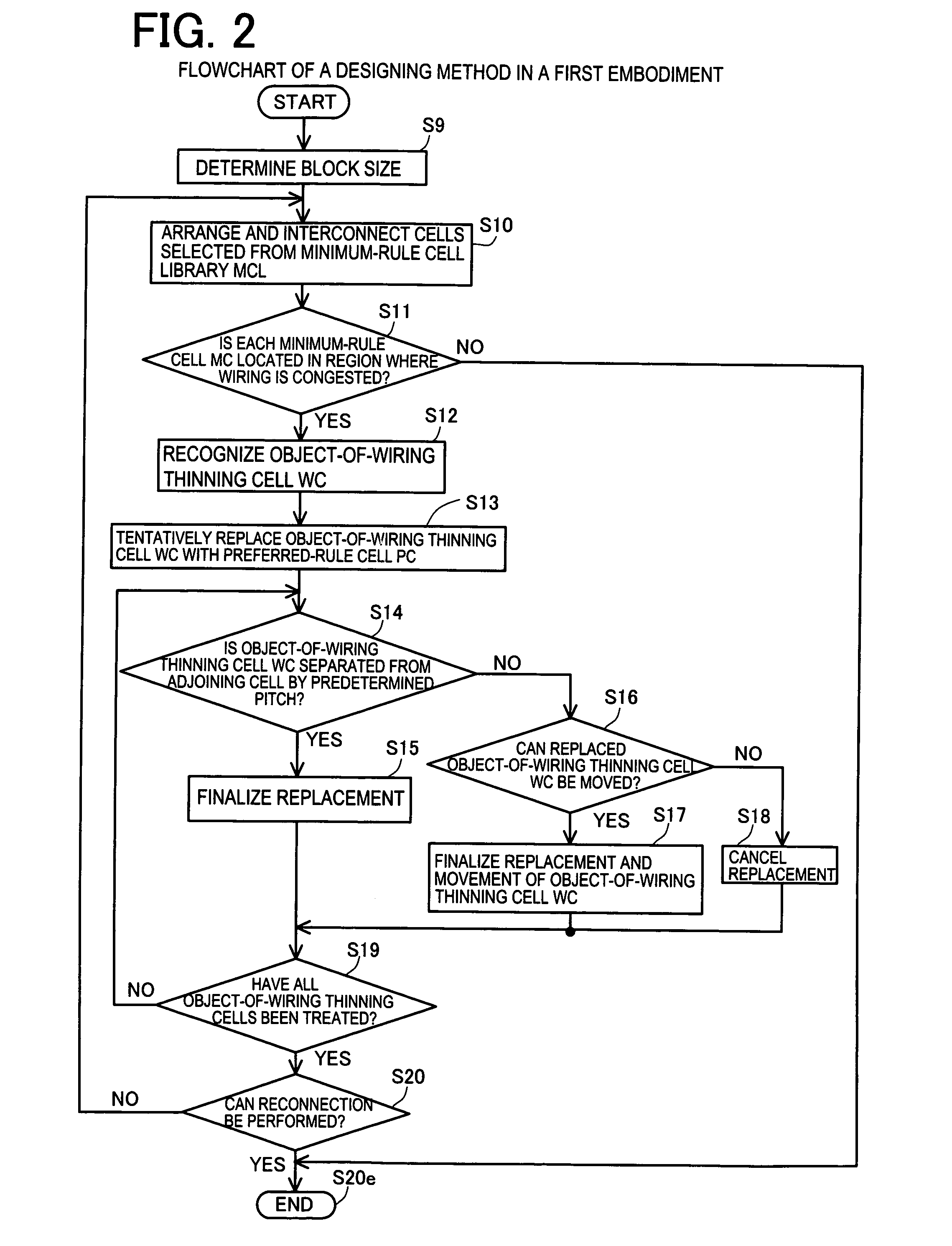
The present invention provides a designing method for a semiconductor integrated circuit that can prevent congestion of wiring and improve yield and signal transmission speed. The method involves arranging and interconnecting cells from two libraries, one containing standard cells and the other containing cells with loosened rules for designing. The method also includes steps of calculating wiring density, replacing an object-of-wiring thinning cell with another cell, and performing reconnection. The invention aims to improve the properties of a cell by reducing congestion of transistors, increasing manufacturing margin, and reducing wiring capacitance.

Problems solved by technology

Congestion of numerous wirings that are oriented in the same direction cannot be resolved.
This poses a problem in that the time (TAT) required for automatic arrangement and connection cannot be shortened.
Moreover, since how to loosen rules for designing a cell is not described at all, a yield cannot be improved by loosening the rules for designing.
Moreover, since a pitch between adjoining lines is not described at all, a signal transmission speed cannot be improved by reducing a wiring capacitance.

Method used


Image

  • Semiconductor integrated circuit designing method and program
  • Semiconductor integrated circuit designing method and program
  • Semiconductor integrated circuit designing method and program

Examples


first embodiment

[0042] Referring to FIG. 1 to FIG. 13, embodiments of the present invention to be adapted to a semiconductor memory device will be described below. the present invention will be described in conjunction with FIG. 1A to FIG. 5B.

[0043] A semiconductor integrated-circuit device that is a product available in a small lot and in diverse types is requested to be developed for a short period of time and is therefore often designed by an automatic arrangement / connection system including a computer. Among various automatic arrangement / connection methods that are known, a standard cell method is often adopted. According to the standard cell method, the patterns of basic gates or logical circuits whose use frequencies are high are registered as standard cells in a cell library. Based on a netlist concerning a semiconductor integrated-circuit device to be manufactured, the standard cells are arranged and interconnected. Thus, automatic arrangement and designing are completed. The cells have a w...

second embodiment

[0069] As described above, according to a semiconductor integrated circuit designing method of the second embodiment, when an unconnected state is caused by arranging preferred-rule cells PC, an object-of-movement cell SC is moved in the state of a preferred-rule cell PC or the object-of-movement cell SC is replaced with a minimum-rule cell MC and then moved. Thus, the unconnected state is resolved. Specifically, cells including terminals that should be connected to each other are moved to approach each other and then moved to a region in which wiring is not congested. Thus, a channel is reserved, and the unconnected state is resolved. Moreover, an obstacle cell that hinders connection of terminals that should be connected to each other is moved in order to reserve a channel. Thus, the unconnected state may be resolved. After a preferred-rule cell PC is moved, when it is not separated from an adjoining cell by a predetermined pitch, the preferred-rule cell is replaced with a minimum...

third embodiment

[0079] As described above, according to a semiconductor integrated circuit designing method of the third embodiment, the freedom in moving cells is ensured, calculation employed in automatic arrangement and connection reliably converges, an unconnected state does not occur, and a free region devoid of a cell is utilized most effectively. A cell ratio can be optimized in order to maximize the number of preferred-rule cells PC. A target cell use rate UR is used as an index for optimizing the cell ratio, namely, the cell ratio is determined so that it will meet the target cell use rate UR. Thus, an optimal cell ratio can be determined quickly and readily. Since the cell ratio is optimized, while occurrence of an unconnected state is prevented, improvement of a yield attributable to the fact that the rules for designing are loosened because of the use of preferred-rule cells PC, and reduction in the total time required for automatic arrangement and connection can be maximized.

[0080] A f...


PUM


Abstract

An object of the present invention is to prevent occurrence of an unconnected terminal during arrangement and connection, shorten the time required for automatic arrangement and connection, improve a yield, and improve the properties of a cell. A recognized object-of-wiring thinning cell (minimum-rule cell) is temporarily replaced with a preferred-rule cell. Since a block has a free region devoid of a cell, an event that a replaced preferred-rule cell interferes with an adjoining one and is not separated from the adjoining one by a predetermined pitch will not take place. Even when the replaced cell interferes with the adjoining one, since the block has the free region devoid of a cell, the cell can be moved to a position at which it will not interfere with the adjoining one. An event that the cell is not separated from the adjoining one by the predetermined pitch will not take place. When all object-of-wiring thinning cells have been treated, reconnection is performed. When processing is terminated, a region of the block is modified.

Description

[0001] This application is based upon and claims the benefit of priority from the prior Japanese Patent Application No. 2004-344097 filed on Nov. 29, 2004, the entire contents of which are incorporated herein by reference. BACKGROUND OF THE INVENTION [0002] 1. Field of the Invention [0003] The present invention relates to a semiconductor integrated circuit designing method and program. More particularly, the present invention is concerned with a semiconductor integrated circuit designing method and program that implement automatic arrangement and connection according to a standard cell technique or the like. [0004] 2. Description of Related Art [0005]FIG. 14A shows an example of a standard cell contained in a cell library A, and FIG. 14B shows an example of a standard cell contained in a cell library B. Hatched areas 121 in FIG. 14A and FIG. 14B indicate a first-layer Al line, and blank areas 122 therein indicate a second-layer Al line. FIG. 14A and FIG. 14B are identical to each ot...

Claims


Application Information

Patent Timeline
Patent Type & Authority Applications(United States)
IPC IPC(8): G06F17/50G06F9/45
CPCG06F17/5068G06F30/39
Inventor NISHIWAKI, AKIFUMI
Owner SOCIONEXT INC
Learn More