Bonding apparatus and bonding method

a technology of electrical bonding and apparatus, which is applied in the direction of non-electric welding apparatus, welding apparatus, manufacturing tools, etc., can solve the problems of easy oxidation of the bonding surface, deterioration of the bonding process, and difficulty in locating the bonding region, so as to achieve the effect of convenient positioning of the bonding region

Inactive Publication Date: 2006-06-08
EBARA CORP
View PDF9 Cites 20 Cited by
  • Summary
  • Abstract
  • Description
  • Claims
  • Application Information

AI Technical Summary

Benefits of technology

[0013] In a preferred aspect of the present invention, the bonding apparatus further comprises at least one preliminary chamber, disposed adjacent to the processing chamber, for transferring the workpieces between an atmospheric environment and the processing chamber without exposing the processing chamber to the atmospheric env

Problems solved by technology

The conventional bonding processes have been problematic for the following reasons: According to the sputtering process in which energy particles are forced to impinge on the bonding surface in a vacuum, since the bonding surface of a semiconductor component or the like needs to be treated at a high temperature, the semiconductor component or the like tends to be deteriorated.
In addition, the bonding surface is liable to be

Method used


Image

  • Bonding apparatus and bonding method
  • Bonding apparatus and bonding method
  • Bonding apparatus and bonding method

Examples


second embodiment

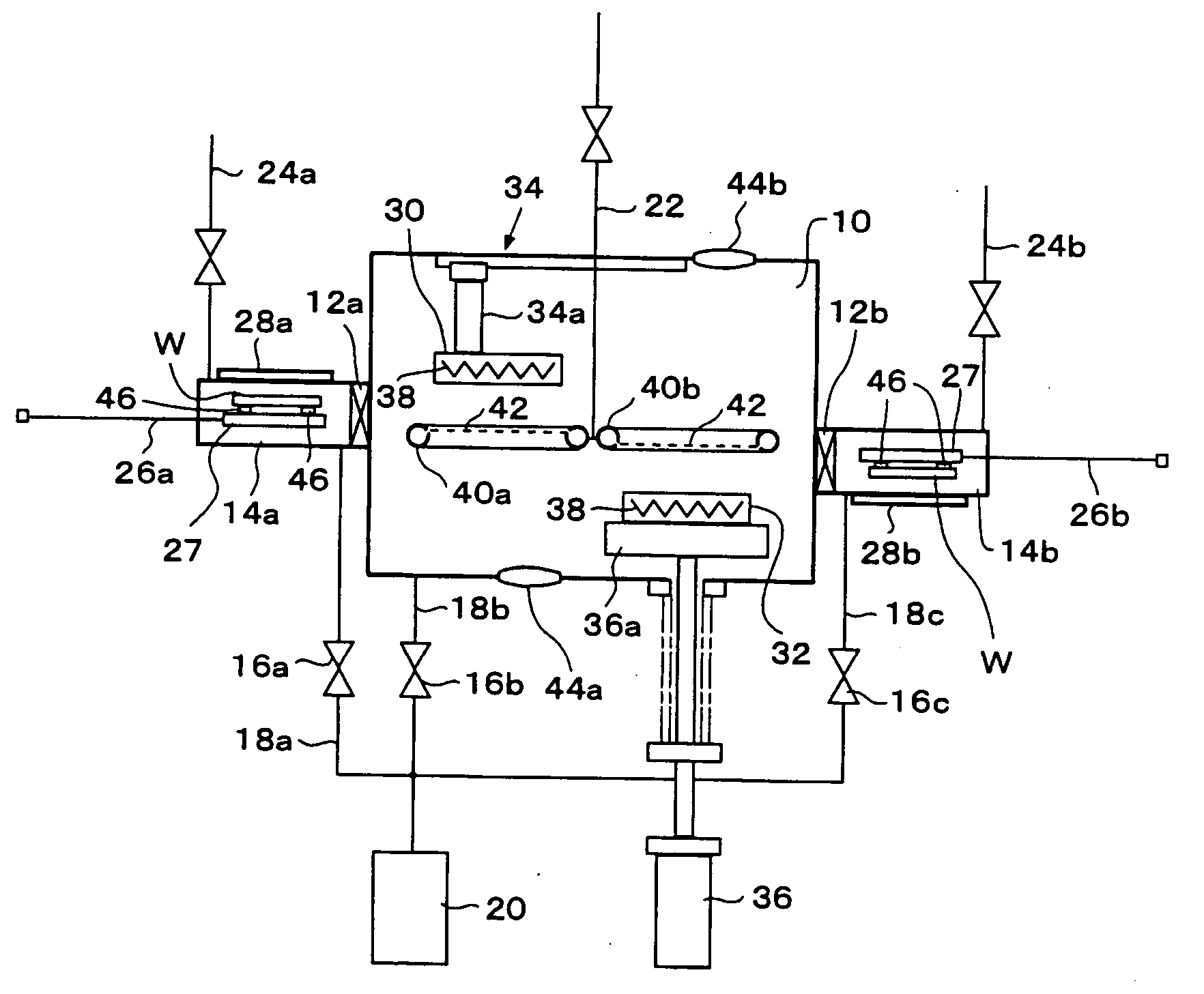
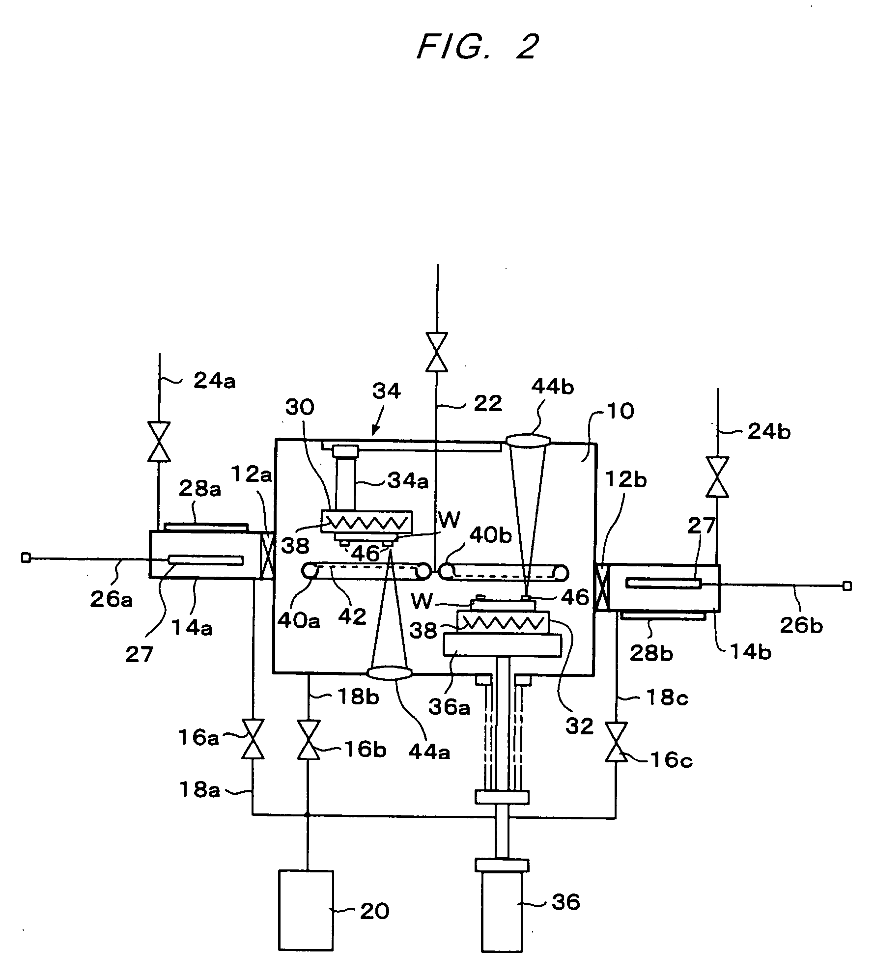
[0052]FIGS. 5 through 7 show a bonding apparatus according to a second embodiment of the present invention. According to the present invention, the workpieces W are positioned outside of the processing chamber. Those parts of the bonding apparatus according to the second embodiment, which are identical or similar to those of the bonding apparatus according to the first embodiment, are denoted by identical or similar reference characters.

[0053] As shown in FIG. 5, a processing chamber 10A houses therein upper and lower support bases 50, 52 which face each other. The support bases 50, 52 do not move horizontally. The lower support base 52 is vertically movable by the pressing mechanism (bonding unit) 36. The processing chamber 10A also houses therein a single gas ejection head 40A having a plurality of horizontal ejection ports 42A. However, the ejection ports 42A may be oriented obliquely in upward and downward directions.

[0054] According to this embodiment, bases 30A, 32A are not f...


PUM

PropertyMeasurementUnit
Temperatureaaaaaaaaaa
Pressureaaaaaaaaaa

Abstract

A bonding apparatus can bond contacts of electronic components directly to each other without the need for solder. The bonding apparatus include a hermetically sealed processing chamber, a plurality of bases for holding at least two workpieces having respective bonding regions in the processing chamber, a gas inlet for introducing a processing gas to clean the bonding regions into the processing chamber, a pressure controller for controlling a predetermined pressure to be developed in the processing chamber, a heater for heating the workpieces in the processing chamber, and a bonding unit for pressing and bonding the bonding regions of the workpieces to each other in the processing chamber.

Description

BACKGROUND OF THE INVENTION [0001] 1. Field of the Invention [0002] The present invention relates to an apparatus for and a method of electrically bonding electronic components, for example. [0003] 2. Description of the Related Art [0004] One device used in fabricating highly integrated semiconductor devices is an interposer module comprising a semiconductor substrate and an interposer substrate that are stacked together. Heretofore, it has been customary to electrically connect such an interposer module with bumps of lead solder formed on contacts. However, efforts have been made in the art to eliminate lead solder for the purpose of reducing environmental burdens. In addition, there have been needs in the art for solder-free bonding to achieve cost reductions by way of material and process cutbacks. [0005] According to a reported solder-free bonding process, a bonding surface of a semiconductor component or the like is physically or chemically cleaned to activate an atomic layer t...

Claims


Application Information

Patent Timeline
IPC IPC(8): B23K1/00B23K5/00B23K20/14
CPCB23K20/023B23K2201/40B23K2101/40
Inventor CHIKAMORI, YUSUKEOGURE, NAOAKITATEISHI, HIDEKIFUKUNAGA, YUKIOUEYAMA, HIROYUKI
Owner EBARA CORP
Why Eureka
Try Eureka