Semiconductor device including field-effect transistor

a field-effect transistor and semiconductor technology, applied in the direction of semiconductor devices, basic electric elements, electrical equipment, etc., can solve the problems of increasing the circuit design effort, affecting the process, and unable to use conventional circuit design

Inactive Publication Date: 2006-06-08
KK TOSHIBA
View PDF24 Cites 36 Cited by
  • Summary
  • Abstract
  • Description
  • Claims
  • Application Information

AI Technical Summary

Benefits of technology

[0021]FIG. 2 is a graph showing the relationship between the uniaxial stress in the channel length direction and the hole mobility at small device of the first to a fourth embodiment of the present invention;
[0022]FIG. 3 is a graph showing the relationship between the uniaxial stress in the channel length direction and the electron mobility at small device of the first to a fourth embodiment of the present invention;

Problems solved by technology

Unfortunately, the above-mentioned methods of changing the plane orientation of the substrate, changing the channel direction, and applying lattice strain have the following problems.
In addition, since rotational symmetry of order four on the wafer cannot be presented, a conventional circuit design cannot be used.
This greatly increases the circuit design effort.
This complicates the process.
This also complicates the process.
In future generations in which the yield presumably lowers due to the progress of micropatterning, it is extremely difficult to use a complicated process in order to increase the mobility.

Method used


Image

  • Semiconductor device including field-effect transistor
  • Semiconductor device including field-effect transistor
  • Semiconductor device including field-effect transistor

Examples


first embodiment

[0031] First, a pMOS transistor and nMOS transistor included in a semiconductor device of a first embodiment of the present invention will be explained.

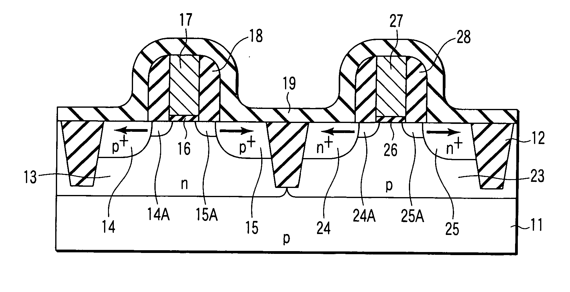
[0032]FIG. 1 is a sectional view showing the structure of the semiconductor device of the first embodiment.

[0033] Element isolation regions 12 are arranged in a p-type silicon substrate 11. The p-type semiconductor substrate 11 is a (001) wafer. The element isolation regions 12 are made of, e.g., shallow trench isolation (STI) in which a silicon oxide film or the like is buried in trenches formed in the p-type semiconductor substrate 11. The element isolation regions 12 electrically insulate and isolate elements (transistors) formed on the p-type semiconductor substrate 11, thereby defining element regions where these elements are formed.

[0034] The structure of a pMOS transistor will be described below.

[0035] An n-type well region 13 is formed on the p-type silicon semiconductor substrate 11. In the surface region of the n-type w...

second embodiment

[0051] A pMOS transistor and nMOS transistor included in a semiconductor device of a second embodiment of the present invention will be described below. The same reference numerals as in the structure of the first embodiment denote the same parts, so an explanation thereof will be omitted, and only different portions will be described below.

[0052]FIG. 7 is a sectional view showing the structure of the semiconductor device of the second embodiment.

[0053] Element isolation regions formed by STI are arranged in an n-type well region 13 and p-type well region 23 on a p-type silicon semiconductor substrate 11. This STI is obtained by burying a silicon nitride film 12A and silicon oxide film 12B in trenches formed in the semiconductor substrate 11 or in the n-type well region 13 and p-type well region 23. The STI has the following structure. The trenches are formed in the p-type silicon semiconductor substrate 11, and the silicon nitride film 12A is formed on those inner surfaces of the...

third embodiment

[0061] A PMOS transistor and nMOS transistor included in a semiconductor device of a third embodiment of the present invention will be described below. The same reference numerals as in the structure of the first embodiment denote the same parts, so an explanation thereof will be omitted, and only different portions will be described below.

[0062]FIG. 10 is a sectional view showing the structure of the semiconductor device of the third embodiment.

[0063] A gate insulating film 16 is formed on an n-type well region 13 between a source region 14 and drain region 15, and a gate electrode 29 is formed on the gate insulating film 16. Also, a gate insulating film 26 is formed on a p-type well region 23 between a source region 24 and drain region 25, and a gate electrode 30 is formed on the gate insulating film 26.

[0064] The gate electrodes 29 and 30 are made of, e.g., polysilicon. A predetermined impurity (e.g., arsenic [As] or germanium [Ge]) by which this polysilicon expands upon annea...


PUM


Abstract

A semiconductor device includes a semiconductor region, source and drain regions, gate insulating film, and gate electrode. The semiconductor region has a plane orientation of (001). The source and drain regions are formed away from each other in the semiconductor region, and a channel region is formed in the semiconductor region between the source and drain regions. The channel length direction of the channel region is set along the direction of <100> of the semiconductor region. Tensile stress is produced in the channel length direction. The gate insulating film is formed on the semiconductor region between the source and drain regions. The gate electrode is formed on the gate insulating film.

Description

CROSS-REFERENCE TO RELATED APPLICATIONS [0001] This application is based upon and claims the benefit of priority from prior Japanese Patent Application No. 2004-355775, filed Dec. 8, 2004, the entire contents of which are incorporated herein by reference. BACKGROUND OF THE INVENTION [0002] 1. Field of the Invention [0003] The present invention relates to a semiconductor device used in, e.g., a complementary metal oxide film semiconductor (CMOS). [0004] 2. Description of the Related Art [0005] To increase the mobility of a p-channel MOS field-effect transistor (referred to as a pMOS transistor hereinafter) and an n-channel MOS field-effect transistor (referred to as an nMOS transistor hereinafter) forming a CMOS, the plane orientation of the substrate or the channel direction is changed, or lattice strain is applied. For example, a silicon-germanium layer serving as a channel increases the hole mobility by compressive stress in the pMOS transistor, and a silicon layer serving as a ch...

Claims


Application Information

Patent Timeline
Patent Type & Authority Applications(United States)
IPC IPC(8): H01L29/94
CPCH01L21/823807H01L21/823814H01L29/1608H01L29/66628H01L29/66636H01L29/7848H01L29/7843H01L21/18
Inventor KOMODA, TAIKI
Owner KK TOSHIBA
Why Eureka
Try Eureka