Semiconductor device, semiconductor module employing thereof and method for manufacturing semiconductor device

a semiconductor module and semiconductor technology, applied in semiconductor devices, semiconductor/solid-state device details, electrical apparatus, etc., can solve the problems of difficult reduction of parasitic capacitance, difficult to provide an improvement in the density of the arrangement plug, and difficult to provide an improved arrangement density of the chip, so as to enhance the degree of integration of the electrically conducting plug. the effect of improving the degree of integration

Inactive Publication Date: 2006-06-08
RENESAS ELECTRONICS CORP
View PDF26 Cites 102 Cited by
  • Summary
  • Abstract
  • Description
  • Claims
  • Application Information

AI Technical Summary

Benefits of technology

[0014] In addition, in this specification, “columnar” for electrically conducting plug indicates a condition where no other material is filled in the interior of the electrically conducting plug. As a typical configuration of “not columnar” may be an annular cylindrical geometry such as an annular cross-sectional geometry. The level of the degree of integration of the electrically conducting plugs can be improved by having the columnar shaped electrically conducting plug. The preferable geometries for enhancing the degree of integration of the electrically conducting plugs therein may include for example, cylinder, cylindroid, or prisms such as quadratic prism octagonal prism and the like. By selecting such geometries, a plurality of electrically conducting plugs can be packed in the through hole at higher density. In addition, the geometry of the electrically conducting plug may be a stripe pattern, in which an electrically conducting film is buried within a slit formed in an insulating film. By selecting such geometry, the configuration allowing efficient filling of the electrically conducting film can be presented.
[0015] According to another aspect of the present invention, there is provided a semiconductor module, comprising a stacked structure of the above-described semiconductor device and other semiconductor device, wherein the plurality of electrically conducting plugs are connected to a conductive member of the other semiconductor device adjacent to the semiconductor device. According to the semiconductor module of the present invention, a plurality of semiconductor devices can be electrically connected at higher density by short distances.
[0018] According to yet other aspect of the present invention, there is provided a method for manufacturing a semiconductor device, comprising: providing a first hole in one surface of a semiconductor substrate and providing a portion of the semiconductor substrate remaining in the inside of the first hole; providing an insulating film on the semiconductor substrate to fill the first hole; providing a plurality of second holes in the portion of the semiconductor substrate remaining in the inside of the first hole from the one surface; forming a first electrically conducting film to fill the plurality of second holes; reducing a thickness of the semiconductor substrate from the other surface of the semiconductor substrate; and exposing the first electrically conducting film.

Problems solved by technology

However, since the technology described in Japanese Patent Laid-Open No. 2003-7,909 utilizes a configuration, in which one plug corresponds to one interconnect, it is difficult to provide an improvement in the density of the arranged plugs.
In addition, a reduction of a parasitic capacitance is difficult.
Further, in the case of semiconductor chip described in Japanese Patent Laid-Open No. 2002-43,502, a region required for disposing one chip through plug is larger, and thus it is difficult to provide an improved arrangement density of the chip through plugs even though a dual ring-shaped slit via is provided.
As described above, these conventional technologies have left rooms for improvement, in view of the difficulty in providing much through electrodes at higher density while achieving the miniaturization of the through electrode.

Method used


Image

  • Semiconductor device, semiconductor module employing thereof and method for manufacturing semiconductor device
  • Semiconductor device, semiconductor module employing thereof and method for manufacturing semiconductor device
  • Semiconductor device, semiconductor module employing thereof and method for manufacturing semiconductor device

Examples


first embodiment

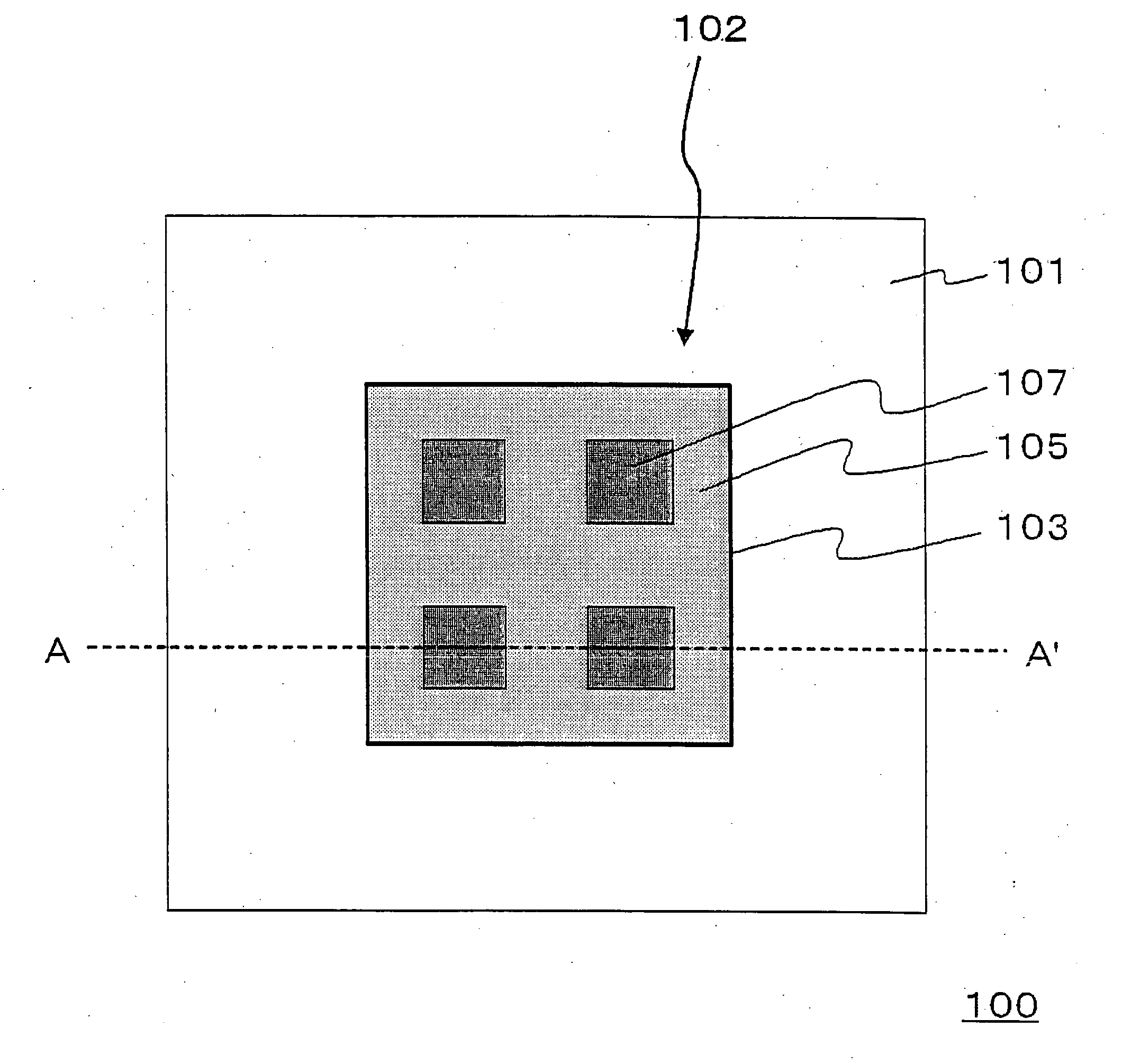
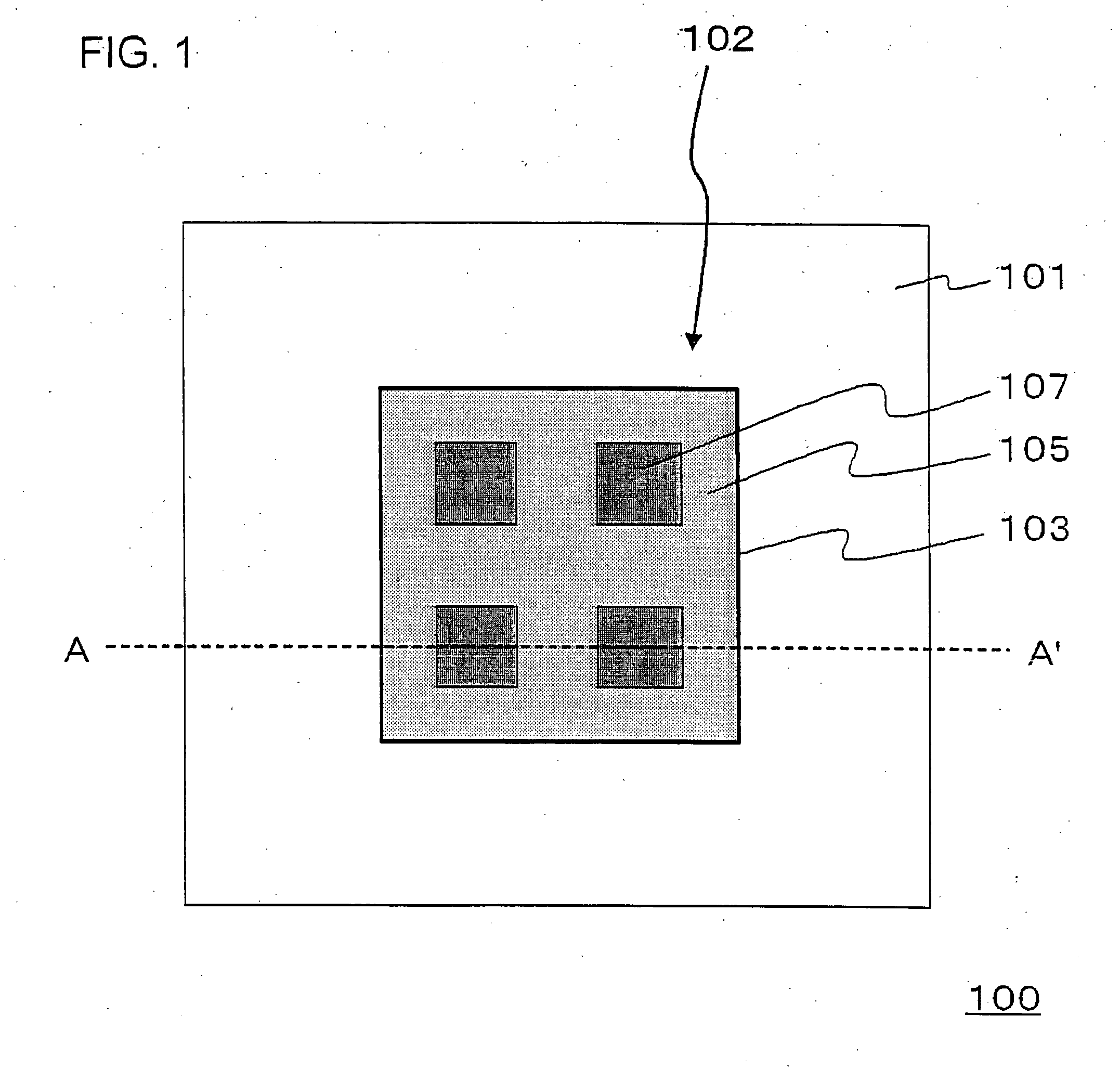
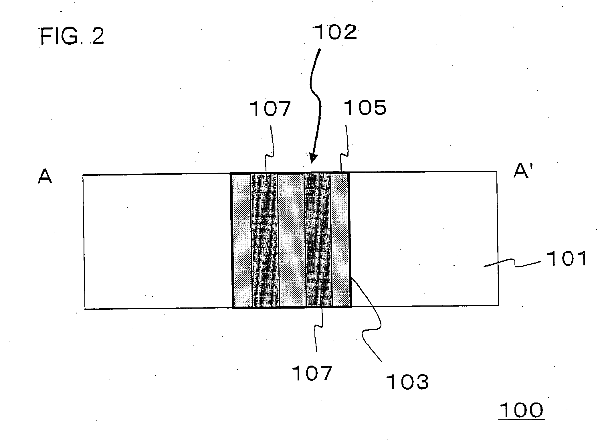
[0067] The present embodiment relates to a semiconductor device that includes a through electrode. FIG. 1 is a diagram, schematically showing a configuration of a semiconductor device according to the present embodiment. FIG. 2 is an cross-sectional view of FIG. 1 along A-A′. The semiconductor device 100 shown in FIG. 1 and FIG. 2 includes a silicon substrate 101, a through hole 103 of having a rectangular cross section extending through the silicon substrate 101, and a through electrode structure 102 that is buried in the through hole 103 and extends through the silicon substrate 101. The through electrode structure 102 includes an insulating film 105 filled in the through hole 103 and a plurality of columnar through plugs 107, each of which is buried in each of a plurality of holes provided in the insulating film 105.

[0068]FIG. 1 illustrates a configuration, in which four through plugs 107 having same cross-sectional geometry of square and same cross sectional area are buried in ...

second embodiment

[0099]FIG. 6 is a plan view, schematically showing a configuration of a semiconductor device according to the present embodiment. A semiconductor device 110 shown in FIG. 6 includes a silicon substrate 101 and a through electrode structure 112. A basic configuration of the through electrode structure 112 is almost similar to the through electrode structure 102 provided in the semiconductor device 100 (FIG. 1) as described in first embodiment, except that a metallic seed layer 115 is provided between the insulating film 105 and the silicon substrate 101. Material for the seed layer 115 may be a metallic material similar to that for the through plug 107, or a metallic material, which is capable of being a nucleus for a metallic plating of through plug 107 and of providing the nuclear growth thereafter. FIG. 7 is an cross-sectional view of FIG. 6 along B-B′.

[0100] Next, the process for manufacturing the semiconductor device 110 shown in FIG. 6 and FIG. 7 will be described. FIGS. 8A to...

third embodiment

[0113] In the present embodiment, a photosensitive material is employed for the material of the insulating film 105 in the semiconductor device described in the above-mentioned embodiment. The semiconductor device 100 described in first embodiment will also be exemplified in this embodiment, as follows.

[0114] Available materials for the insulating film 105 may include photosensitive materials exhibiting an electrical insulation, such as photosensitive glasses, or photopolymers such as photosensitivity polyimide and the like. The photosensitive material may be a positive type, or a negative type. When the insulating film 105 composed of a positive type photosensitive material is employed, the semiconductor device 100 is manufactured in the following procedure.

[0115] First, a concave portion 153 is formed in the silicon substrate 101 by employing the process described above in reference to FIG. 3A. Then, a photosensitive material such as, for example, a film of photosensitivity poly...


PUM


Abstract

The layout density of the through electrodes in the horizontal plane of the substrate is enhanced. Through holes 103 extending through the silicon substrate 101 is provided. An insulating film 105 is buried within the through hole 103. A plurality of columnar through plugs 107 are provided in the insulating film 105.

Description

[0001] This application is based on Japanese patent application No. 2004-349,688, the content of which is incorporated hereinto by reference. BACKGROUND [0002] 1. Technical Field [0003] The present invention relates to a semiconductor device comprising a through electrode, a semiconductor module employing thereof and a method for manufacturing a semiconductor device. [0004] 2. Related Art [0005] In the conventional technology, bare chip stack-type multiple-chip module (MCM) has been proposed for the purpose of achieving higher degree of integration over a system in package (SiP) a type of having arranged chips in parallel or of a package-stack type. An interconnect extending through the semiconductor substrate is essential for the bare chip stack-type module. Exemplary conventional bare chip stack-type MCMs having a through electrode are described in Japanese Patent Laid-Open No. 2003-7,909. [0006] Japanese Patent Laid-Open No. 2003-7,909 describes a semiconductor device comprising ...

Claims


Application Information

Patent Timeline
Patent Type & Authority Applications(United States)
IPC IPC(8): H01L23/48
CPCH01L23/481H01L25/0657H01L2224/16H01L2225/06513H01L2225/06541H01L2924/01077H01L2924/01078H01L2924/01079H01L2924/15311H01L2924/3011H01L2924/3025H01L2224/16145H01L2224/16225H01L2224/0554H01L2224/05573H01L2224/06131H01L2224/13025H01L2924/00014H01L2924/12044H01L2924/00H01L2224/05599H01L2224/0555H01L2224/0556
Inventor MATSUI, SATOSHI
Owner RENESAS ELECTRONICS CORP
Why Eureka
Try Eureka