Active-matrix display device, and active-matrix organic electroluminescent display device
a display device and active matrix technology, applied in the direction of static indicating devices, identification means, instruments, etc., can solve the problems of large variation in tft characteristics, difficult to uniformly irradiate a relatively large-sized glass substrate with laser energy, and the inability to use a large-scale and high-definition display
- Summary
- Abstract
- Description
- Claims
- Application Information
AI Technical Summary
Benefits of technology
Problems solved by technology
Method used
Image

Examples
first embodiment
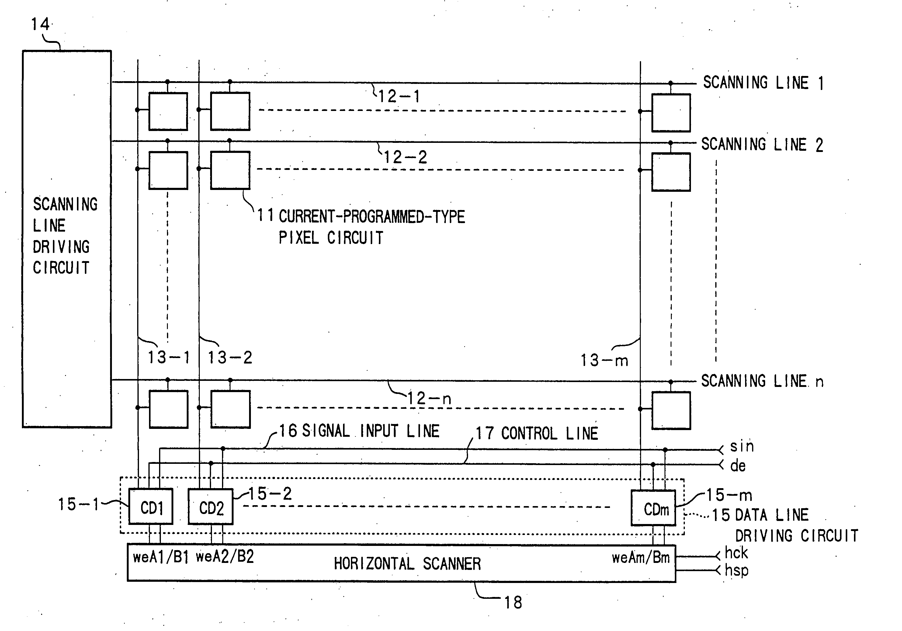
[0081]FIG. 1 is a block diagram showing an example of the configuration of an active-matrix display device according to a first embodiment of the present invention. As shown in FIG. 1, a plurality of pixel circuits 11 is arranged in a matrix, forming a display area (a display unit). The display area includes a matrix of n rows by m columns of pixels. The display area includes n scanning lines 12-1 through 12-n for selecting each pixel (each pixel circuit) and m data lines 13-1 through 13-m for supplying each pixel with image data such as luminance data.
[0082] A scanning line driving circuit 14 for selecting the scanning lines 12-1 through 12-n and a data line driving circuit 15 for driving the data lines 13-1 through 13-m are arranged external to the display area. The scanning line driving circuit 14 is formed of a shift register, for example, and output terminals of stages thereof are respectively connected to the ends of the scanning lines 12-1 through 12-n. As will be discussed ...
first circuit example
[0089]FIG. 4 is a circuit diagram specifically showing one of the current drivers 15-1 through 15-m forming the data line driving circuit 15. All the current drivers 15-1 through 15-m are identical to each other in configuration.
[0090] The current driver in the first embodiment includes four TFTs 31-34, and one capacitor 35. In this circuit example, all the TFTs 31-34 are manufactured of NMOS transistors, but the present invention is not limited this type of transistor.
[0091] In FIG. 4, the TFT 31 with the source thereof grounded functions as a converting unit. The drain of the TFT 31 are the sources of the TFT 32 and the TFT 33, and the drain of the TFT 34. The TFT 32 is a first switching element with the drain thereof connected to the signal input line 16, and with the gate thereof receiving a first writing control signal weA. The TFT 33 with the drain thereof connected to a data line 13 functions as a driving unit, and receives, at the gate thereof, a driving control signal de ...
second circuit example
[0104]FIG. 6 is a circuit diagram showing another circuit example of the current drivers 15-1 through 15-m. In the figure, the same parts as those of FIG. 4 are indicated by the same symbols as those of FIG. 4.
[0105] The current driver of this example further includes, besides the circuit elements shown in FIG. 4, an impedance transforming Transistor, that is a PMOS type TFT 40 having a different conductive type from that of the TFT 31, arranged between the TFT 31 and the current source CS, and operating in the saturation region thereof during the writing of the luminance data sin. The impedance transforming TFT 40 is actually connected to the TFT 31 through the TFT 32. With this arrangement, the writing of the luminance data sin onto the current driver is performed faster than the circuit shown in FIG. 4. The reason for this will be discussed.
[0106] In the current writing, there is a problem that the time required to the writing is typically longer. When the current Iw is written...
PUM
 Abstract
Description
Claims
Application Information
 - Generate Ideas
- Intellectual Property
- Life Sciences
- Materials
- Tech Scout
- Unparalleled Data Quality
- Higher Quality Content
- 60% Fewer Hallucinations
Browse by: Latest US Patents, China's latest patents, Technical Efficacy Thesaurus, Application Domain, Technology Topic, Popular Technical Reports.
© 2025 PatSnap. All rights reserved.Legal|Privacy policy|Modern Slavery Act Transparency Statement|Sitemap|About US| Contact US: help@patsnap.com