OLED displays with varying sized pixels

a technology of oled displays and pixels, applied in the field of oled displays, can solve the problems of undesirable bending of signal lines, impracticality of approaching, signal lines becoming bent, etc., and achieve the effect of reducing resistance and less surface area

Active Publication Date: 2006-06-08
GLOBAL OLED TECH
View PDF19 Cites 46 Cited by
  • Summary
  • Abstract
  • Description
  • Claims
  • Application Information

AI Technical Summary

Benefits of technology

[0020] The invention has the advantage over prior OLED active matrix display designs that pixels having differing colors can be located in both the same row and column and can be optimized to have differing emitting area sizes having differing heights and widths. The invention also has the advantage that signal lines have reduced resistance and require less surface area.

Problems solved by technology

Bending the signal lines is undesirable because bent signal lines are effectively longer and therefore more resistive.
However, when applied to other patterns in which differently colored pixels are located in the same rows and columns, this approach becomes impractical.
However, routing the signal lines around the emitting regions of the pixels results in the signal lines becoming bent as describe above.

Method used


Image

  • OLED displays with varying sized pixels
  • OLED displays with varying sized pixels
  • OLED displays with varying sized pixels

Examples


first embodiment

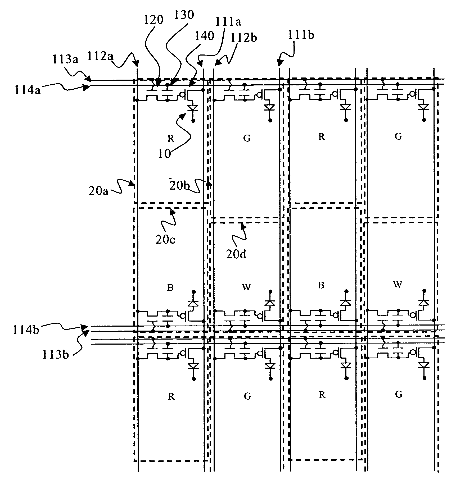
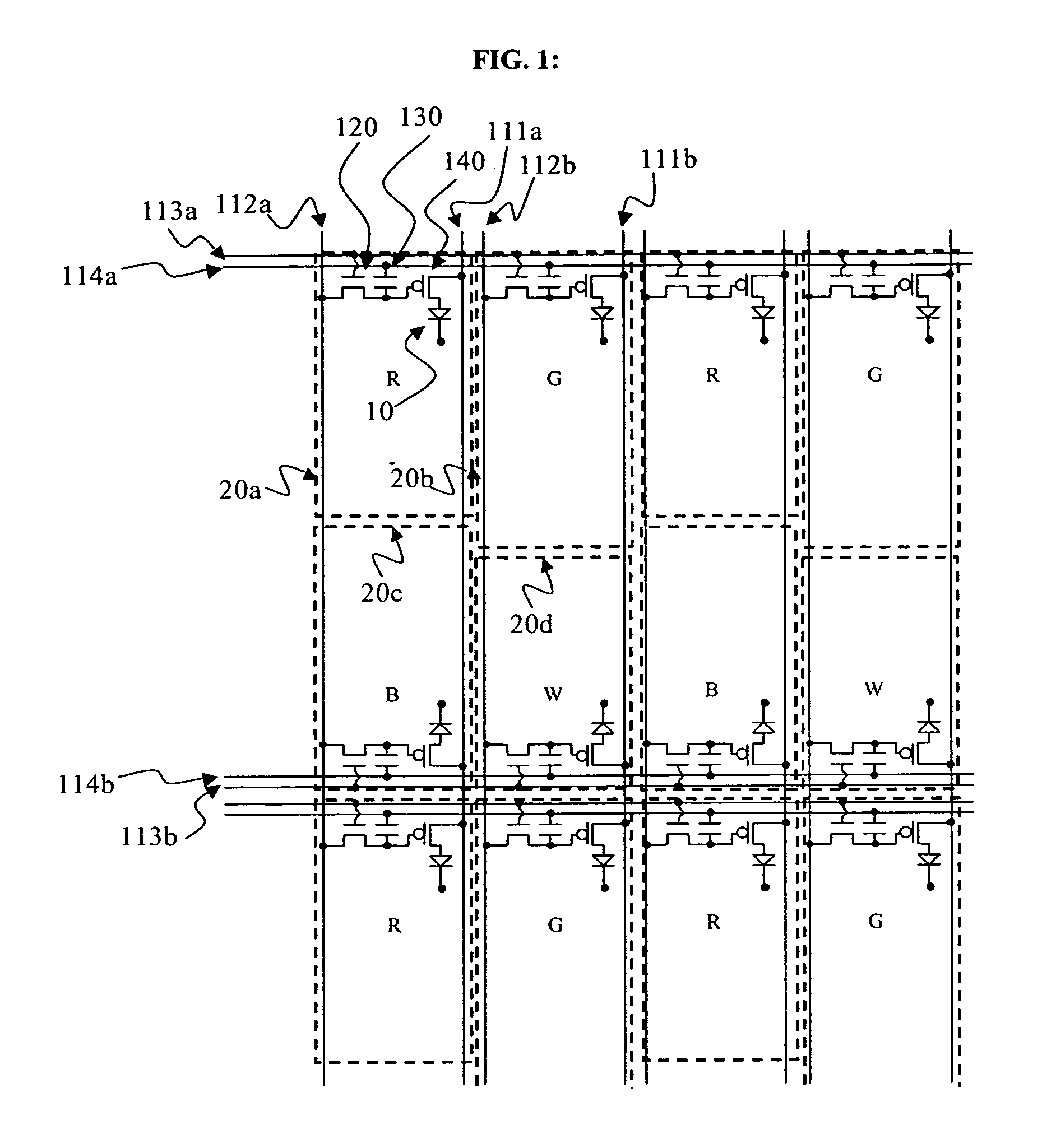
[0035] The emitting areas of the pixels can be adjusted without bending of any of the signal lines by adjusting the size of the emitting area in the column direction, or height (H), or adjusting the size of the emitting area in the row direction, or width (L). According to the present invention, by disposing select line 113a and select line 113b on the outside of their associated pixels, different heights of the pixel emitting areas can be achieved for pixels in the same row, as shown. That is, the emitting areas of pixels 20a, 20b, 20c, and 20d are disposed between select line 113a and select line 113b, permitting the select lines to be formed in a linear, unbending, fashion. That is, a signal line, such as the select line, are considered to be linear if they form a straight path between all the pixels connected to the signal line. The signal line may vary in width along its length and still be considered linear. Therefore by providing the select lines of these two adjacent rows of...

second embodiment

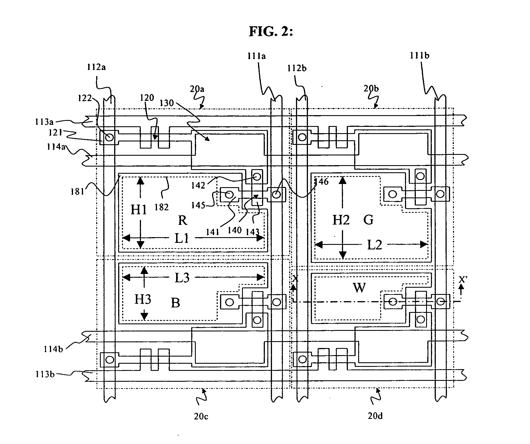
[0052] By forming a display according to the second layout embodiment, the emitting areas of the pixels can be adjusted without bending of any of the signal lines by adjusting the size of the emitting area in the column direction, or height (H), or adjusting the size of the emitting area in the row direction, or width (L). According to the present invention, different heights of the pixel emitting areas can be achieved for pixels in the same row and different widths of the pixel emitting area can be achieved for pixels in the same column, as shown. That is, the emitting areas of pixels 20a, 20b, 20c, and 20d are disposed between select line 113a and select line 113b, between power line 111a and power line 111b, and between data line 112a and data line 112b, permitting these signal lines to be formed in a linear, unbending, fashion. Therefore, pixels in the same row may be provided with different heights, such as height H6 of pixel 20d and height H7 of pixel 20c. Pixels in the same r...


PUM


Abstract

An active matrix OLED display has pixels with light emitting areas arranged in rows and columns and includes; a first pixel having a first height in the column direction and disposed in a first column of pixels and in a first row of pixels; a second pixel having a second height in the column direction and disposed in the first column of pixels and in a second row of pixels wherein the second row of pixels is adjacent to the first row of pixels and the first height being different than the second height; and a first select line arranged to drive only the first row of pixels and a second select lines spaced from the first select line arranged to drive only the second row of pixels wherein the emitting areas of the first and second pixels are disposed between the first and second select lines.

Description

FIELD OF THE INVENTION [0001] The present invention relates to OLED displays having different sized pixels. BACKGROUND OF THE INVENTION [0002] In the simplest form, an organic electroluminescent (EL) device is comprised of an anode for hole injection, a cathode for electron injection, and an organic media sandwiched between these electrodes to support charge recombination that yields emission of light. These devices are also commonly referred to as organic light emitting diodes, or OLEDs. A basic organic EL element is described in U.S. Pat. No. 4,356,429. In order to construct a pixelated OLED display such as is useful as a display such as, for example, a television, computer monitor, cell phone display, or digital camera display, individual organic EL elements can be arranged as pixels in a matrix pattern. These pixels can all be made to emit the same color, thereby producing a monochromatic display, or they can be made to produce multiple colors such as a red, green, blue (RGB) di...

Claims


Application Information

Patent Timeline
Patent Type & Authority Applications(United States)
IPC IPC(8): G09G3/32
CPCG09G3/3225G09G2300/0452G09G2300/0842H01L27/3213H01L27/3244H01L27/3216H10K59/351H10K59/352H10K59/12
Inventor WINTERS, DUSTIN L.VAN SLYKE, STEVEN A.
Owner GLOBAL OLED TECH
Why Eureka
Try Eureka