
Electronic device and method of using the same

Inactive Publication Date: 2006-06-08
EI DU PONT DE NEMOURS & CO
View PDF24 Cites 40 Cited by
  • Summary
  • Abstract
  • Description
  • Claims
  • Application Information

AI Technical Summary

Benefits of technology

[0129] One or more embodiments described herein can be used to help to extend the useful life of electronic devices. The calibration techniques generate as little as one calibration value for the entire array or for any portion thereof. Because calibration data is not being collected on a pixel-by-pixel basis, the calibration procedure can be performed more quickly and does not need as much memory. Similarly, as little as one adjustment factor may be used for the entire array or for any portion thereof. Because adjustment factor(s) are not applied on a pixel-by-pixel basis, not as much memory is needed. The calibration and normal (e.g., display) modes may be performed faster and at lower power (due to less data being stored and retrieved).
[0130] In a full-color display, every pixel contains three sub-pixels emitting red, green or blue colors respectively. The three-color subpixel sets could have different aging mechanisms or different aging rates. The calibration procedure above could be extended into the three primary color emitter sets. When the intensities of sub-pixels within the emitter set are calibrated, the white color balance of the full-color disp

Problems solved by technology

Due to a degradation of the radiation-emitting properties of organic electroluminescent materials over the operation lifetime of an OLED, long time operation with a stationary image can result in a burned-in pattern on the display, which reduces display quality considerably.
The driving scheme described in the patent publication may have a relatively high cost, and therefore, may be limited to only certain applications.
For many other applications, such a driving scheme may be viewed as too complicated, too costly, or both.

Method used


Image

  • Electronic device and method of using the same
  • Electronic device and method of using the same
  • Electronic device and method of using the same

Examples


example 1

[0134] Example 1 illustrates that the compensation devices and methods can be used to achieve more constant emission intensity during the lifetime of radiation-emitting electronic components. Two OLEDs comprising polymer active layers are fabricated using conventional procedures. Glass / ITO is used as substrate and transparent anode. A thin layer of polyaniline or poly(3,4-ethylendioxythiophene) (“PEDOT”) is deposited over the glass / ITO. A polyfluorene-based organic active layer is then deposited over the thin layer of polyaniline or PEDOT. A thin layer of metal Ba / Al is vacuum deposited over top of polyfluorene organic layer and serves as a cathode. The color of radiation emitted from the electronic devices depends on the opto-electronic properties of the material(s) within the organic active layer. One electronic device is operated using a conventional driving scheme, i.e. constant current at approximately 7 mA. The other electronic device is operated using a compensation driving s...

example 2

[0135] Example 2 demonstrates that the methods disclosed herein do not only compensate the electronic component aging, but also compensate the maximum intensity variation caused by other sources, such as from aging of electronic components within pixel driver circuits. Example 2 also illustrates that the configuration as illustrated in FIG. 8 can be used to measure radiation intensity for a 10×10 matrix OLED display. In one embodiment, the matrix is an active matrix, and in another embodiment, the matrix is a passive matrix.

[0136]FIG. 15 includes a circuit diagram of an electronic device 1500 that includes a power transistor 1502, a capacitive electronic component 1504, a switch 1506, and an organic electronic component 1508. The organic electronic component 1508 may be a radiation-emitting electronic component, a radiation-sensing electronic component, or the like. In one embodiment, the electronic device 1500 includes an array of the circuits as illustrated in FIG. 15. Each of th...

example 3

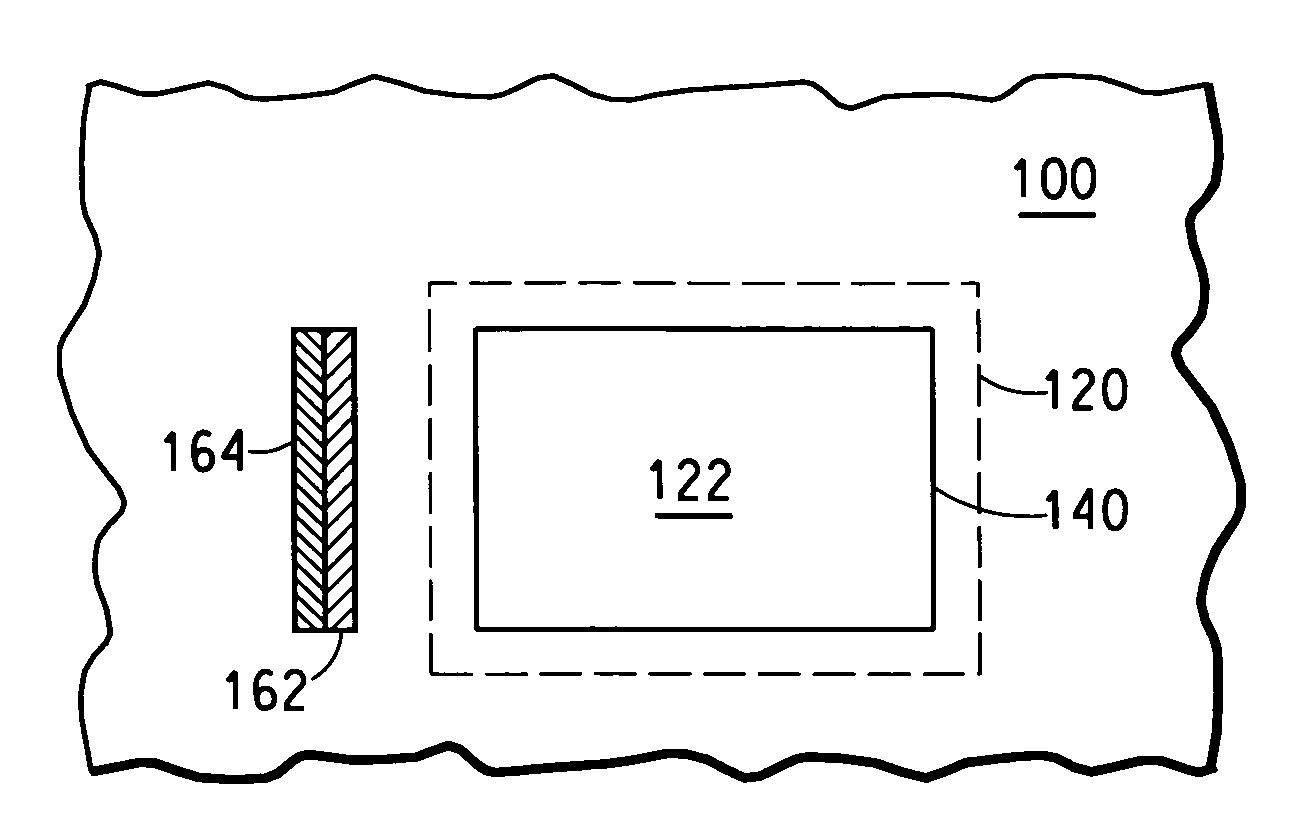
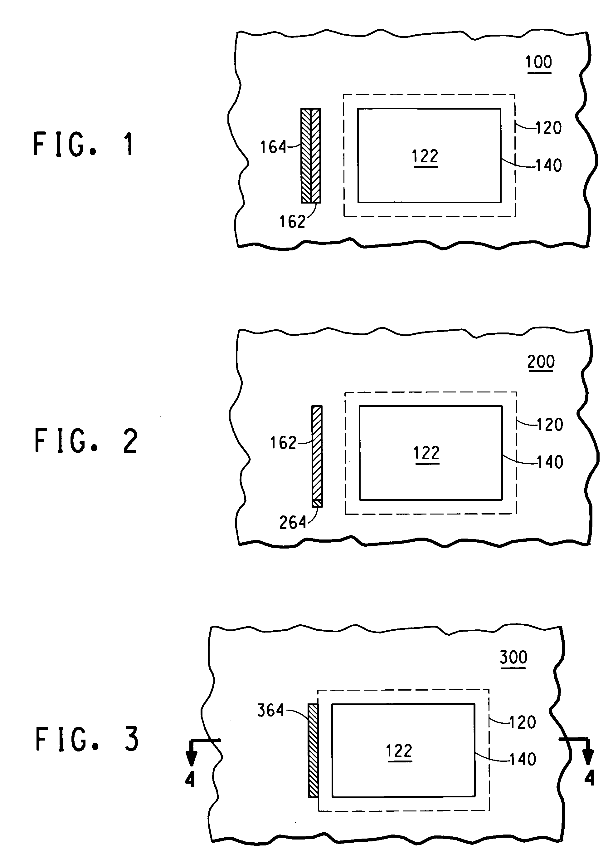
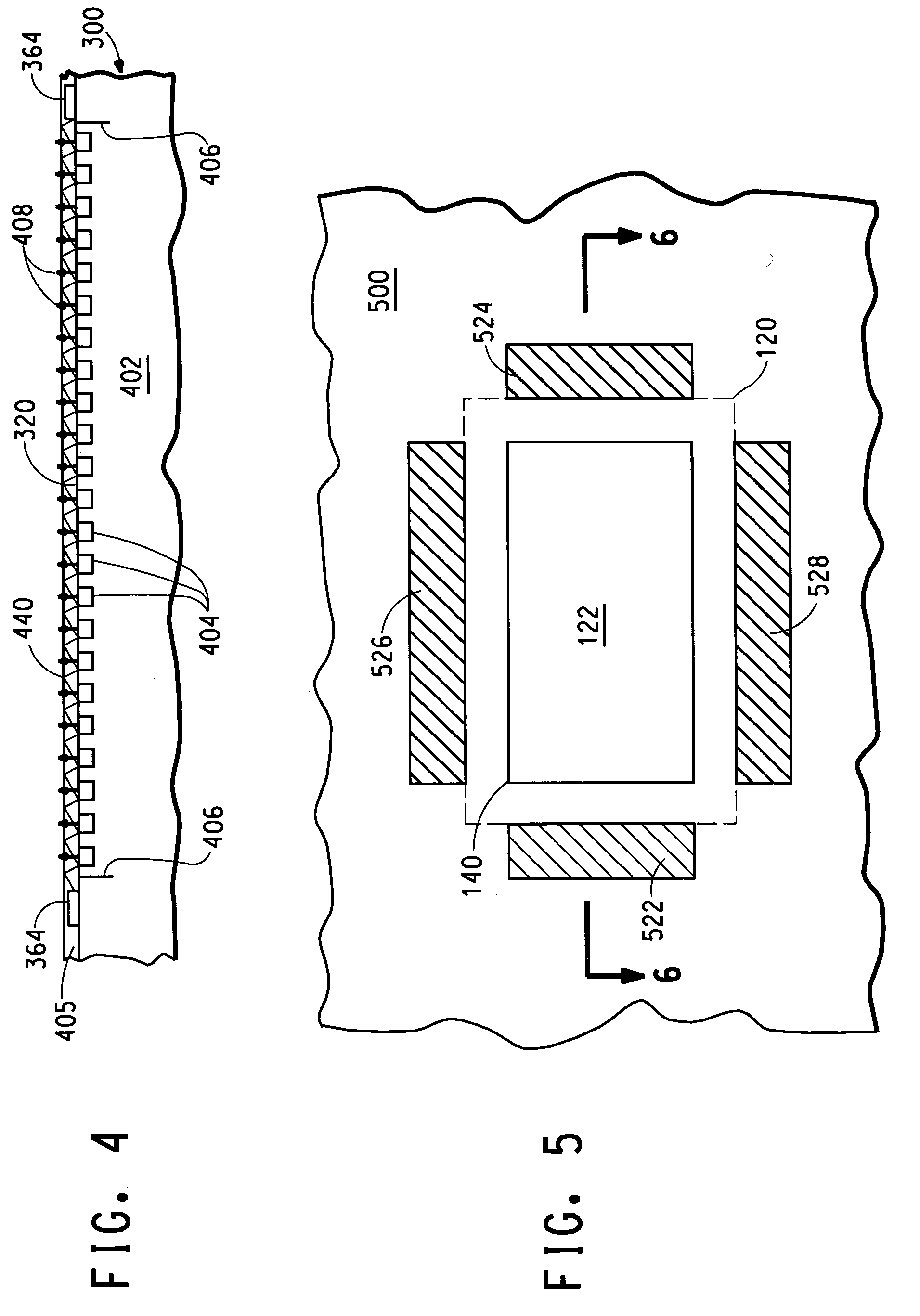
[0149] Example 3 demonstrates that the compensation scheme and apparatus disclosed in FIGS. 1 and 2 are practical for AMOLED displays and provide stable maximum emission intensity. The electronic device in this example includes a 4″ (nominal) AMOLED user display with a QVGA format (320×RGB×240 pixels). The electronic device also includes 10×RGB columns on each side of the display as dummy displays. The dummy displays are operated with the same data signal as the center portion of the user display. The maximum emission intensity of the dummy displays are measured during predetermined periods, and the variation is used to adjust the emission intensity of both the dummy and user displays. Stable maximum emission intensities can be achieved in both dummy and user displays.


PUM


Abstract

An electronic device includes a data processing system and a set of pixels that each include one or more radiation-emitting electronic components, one or more radiation-sensing electronic components, or any combination thereof. The data processing system that is configured to access data regarding the set of pixels and determine at least one calibration value corresponding to the data. The number of the calibration value(s) is less than the number of the pixels within the set. The data processing system is further configured to compare the calibration value(s) to another value and change at least one adjustment factor if the calibration value(s) differs from the other value by more than a predetermined amount. The number of the adjustment factor(s) is less than the number of the pixels within the set. Data processing system readable media and methods for using the electronic device are also described.

Description

BACKGROUND OF THE INVENTION [0001] 1. Field of the Invention [0002] This invention relates in general to electronic devices, and more particularly, to electronic devices including radiation-emitting electronic components and methods of using the same. [0003] 2. Description of the Related Art [0004] Organic electronic devices have attracted considerable attention in recent years. Examples of organic electronic devices include Organic Light-Emitting Diodes (“OLEDs”), which include Polymer Light-Emitting Diodes (“PLEDs”) and Small Molecule Organic Light-Emitting Diodes (“SMOLEDs”). [0005] Due to a degradation of the radiation-emitting properties of organic electroluminescent materials over the operation lifetime of an OLED, long time operation with a stationary image can result in a burned-in pattern on the display, which reduces display quality considerably. Two approaches can be used to eliminate this image retention: (1) developing new materials and (2) implementing a compensation m...

Claims


Application Information

Patent Timeline
IPC IPC(8): G09G5/00H05B44/00
CPCG09G3/3216G09G3/3258G09G2300/0842G09G2320/0242G09G2320/029G09G2320/043G09G2320/0606G09G2320/0626G09G2320/0693G09G2360/145G09G3/20G09G3/30
Inventor WANG, JIANZHANG, WEIXIAOYU, GANG
Owner EI DU PONT DE NEMOURS & CO
Learn More