System and driving method for active matrix light emitting device display

a technology of light emitting devices and driving methods, which is applied in the direction of static indicating devices, instruments, etc., can solve the problems of increasing the settling time of the current-programmed amoled display programming, difficult to design external drivers to accurately supply the required current, and unsatisfactory results

Active Publication Date: 2006-06-15
IGNIS INNOVATION
View PDF10 Cites 97 Cited by
  • Summary
  • Abstract
  • Description
  • Claims
  • Application Information

AI Technical Summary

Benefits of technology

[0006] It is an object of the invention to provide a method and system that obviates or mitigates at least one of the disadvantages of existing systems.

Problems solved by technology

However, the small current required by the OLED, coupled with a large parasitic capacitance, undesirably increases the settling time of the programming of the current-programmed AMOLED display.
Furthermore, it is difficult to design an external driver to accurately supply the required current.
For example, in CMOS technology, the transistors must work in sub-threshold regime to provide the small current required by the OLEDs, which is not ideal.
However, this method is not applicable for other current-programmed pixel circuits.
Also, by resizing the two mirror transistors the effect of mismatch increases.

Method used


Image

  • System and driving method for active matrix light emitting device display
  • System and driving method for active matrix light emitting device display
  • System and driving method for active matrix light emitting device display

Examples


Embodiment Construction

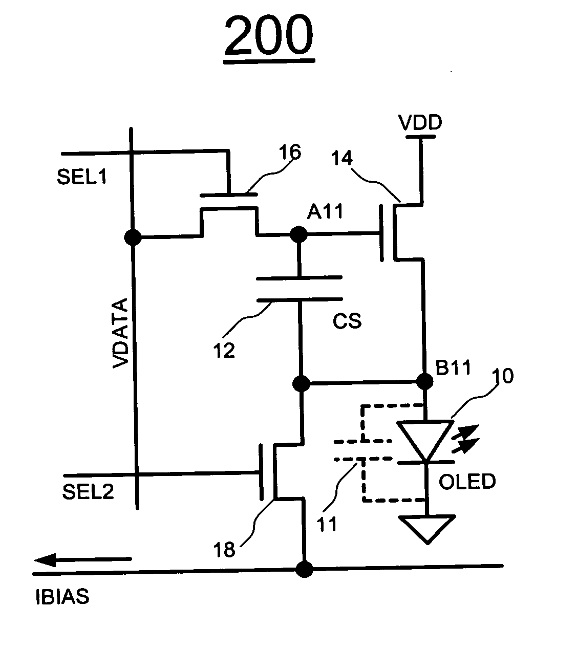
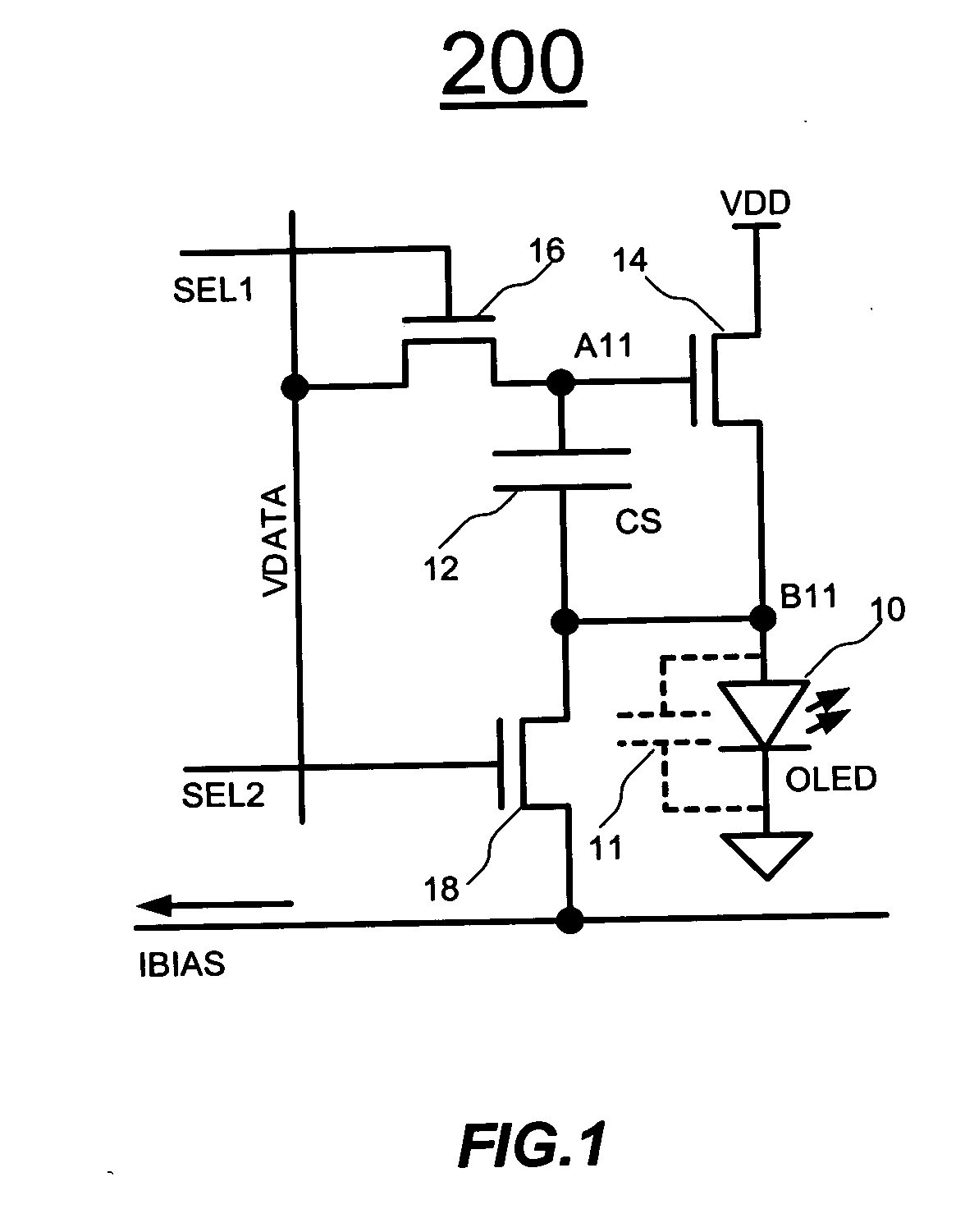
[0035] Embodiments of the present invention are described using a pixel having an organic light emitting diode (OLED) and a driving thin film transistor (TFT). However, the pixel may include any light emitting device other than OLED, and the pixel may include any driving transistor other than TFT. It is noted that in the description, “pixel circuit” and “pixel” may be used interchangeably.

[0036] A driving technique for pixels, including a current-biased voltage-programmed (CBVP) driving scheme, is now described in detail. The CBVP driving scheme uses voltage to provide for different gray scales (voltage programming), and uses a bias to accelerate the programming and compensate for the time dependent parameters of a pixel, such as a threshold voltage shift and OLED voltage shift.

[0037]FIG. 1 illustrates a pixel circuit 200 in accordance with an embodiment of the present invention. The pixel circuit 200 employs the CBVP driving scheme as described below. The pixel circuit 200 of FIG...


PUM


Abstract

Active matrix light emitting device display and its driving technique is provided. The pixel includes a light emitting device and a plurality of transistors. A capacitor may be used to store a voltage applied to a driving transistor so that a current through the light emitting device is independent of any shifts of the transistor and light emitting device characteristics. A bias data and a programming data are provided to the pixel circuit in accordance with a driving scheme.

Description

FIELD OF INVENTION [0001] The present invention relates to a light emitting device displays, and more specifically to a driving technique for the light emitting device displays. BACKGROUND OF THE INVENTION [0002] Recently active-matrix organic light-emitting diode (AMOLED) displays with amorphous silicon (a-Si), poly-silicon, organic, or other driving backplane technology have become more attractive due to advantages over active matrix liquid crystal displays. An AMOLED display using a-Si backplanes, for example, has the advantages which include low temperature fabrication that broadens the use of different substrates and makes flexible displays feasible, and its low cost fabrication is well-established and yields high resolution displays with a wide viewing angle. [0003] An AMOLED display includes an array of rows and columns of pixels, each having an organic light-emitting diode (OLED) and backplane electronics arranged in the array of rows and columns. Since the OLED is a current...

Claims


Application Information

Patent Timeline
Patent Type & Authority Applications(United States)
IPC IPC(8): G09G3/10
CPCG09G3/3233G09G3/3241G09G2300/043G09G2300/0819G09G2300/0842G09G2300/0852G09G2300/0861G09G2310/0251G09G2320/043
Inventor NATHAN, AROKIACHAJI, GHOLAMREZA REZASERVATI, PEYMAN
Owner IGNIS INNOVATION
Why Eureka
Try Eureka