Substrate for use in a liquid crystal display and liquid crystal display using the same
What is AI technical title?
AI technical title is built by Patsnap AI team. It summarizes the technical point description of the patent document.
a liquid crystal display and substrate technology, applied in the direction of optics, transistors, instruments, etc., can solve the problems of intense light leakage from backlight units, cracks, etc., and achieve the effect of suppressing cracks
Inactive Publication Date: 2006-06-15
HOSHINO ATUYUKI +16
View PDF15 Cites 19 Cited by
Summary
Abstract
Description
Claims
Application Information
AI Technical Summary
This helps you quickly interpret patents by identifying the three key elements:
Problems solved by technology
Method used
Benefits of technology
Benefits of technology
This approach enhances the manufacturing process reliability, reduces light leakage, prevents contamination, and maintains uniform cell thickness, achieving high light shielding capability and improved display quality.
Problems solved by technology
When a resin layer is formed on the whole surface of the substrate, and an electrode wiring line made of, for example, a transparent oxideelectrode material or the like is formed on the resin layer, the adhesion of the wiring line or the like to the resin layer is often inferior to that to a glass substrate, and there is a case where peeling occurs.
In the CF-on-TFT structure in which the opposite electrode does not have a light shielding film, an intense light leakage from a backlight unit is problematic in the frame region of the periphery of a display region.
Method used
Image
Click on the blue label to locate the original text in one second.
Reading with bidirectional positioning of images and text.
Examples
Embodiment Construction
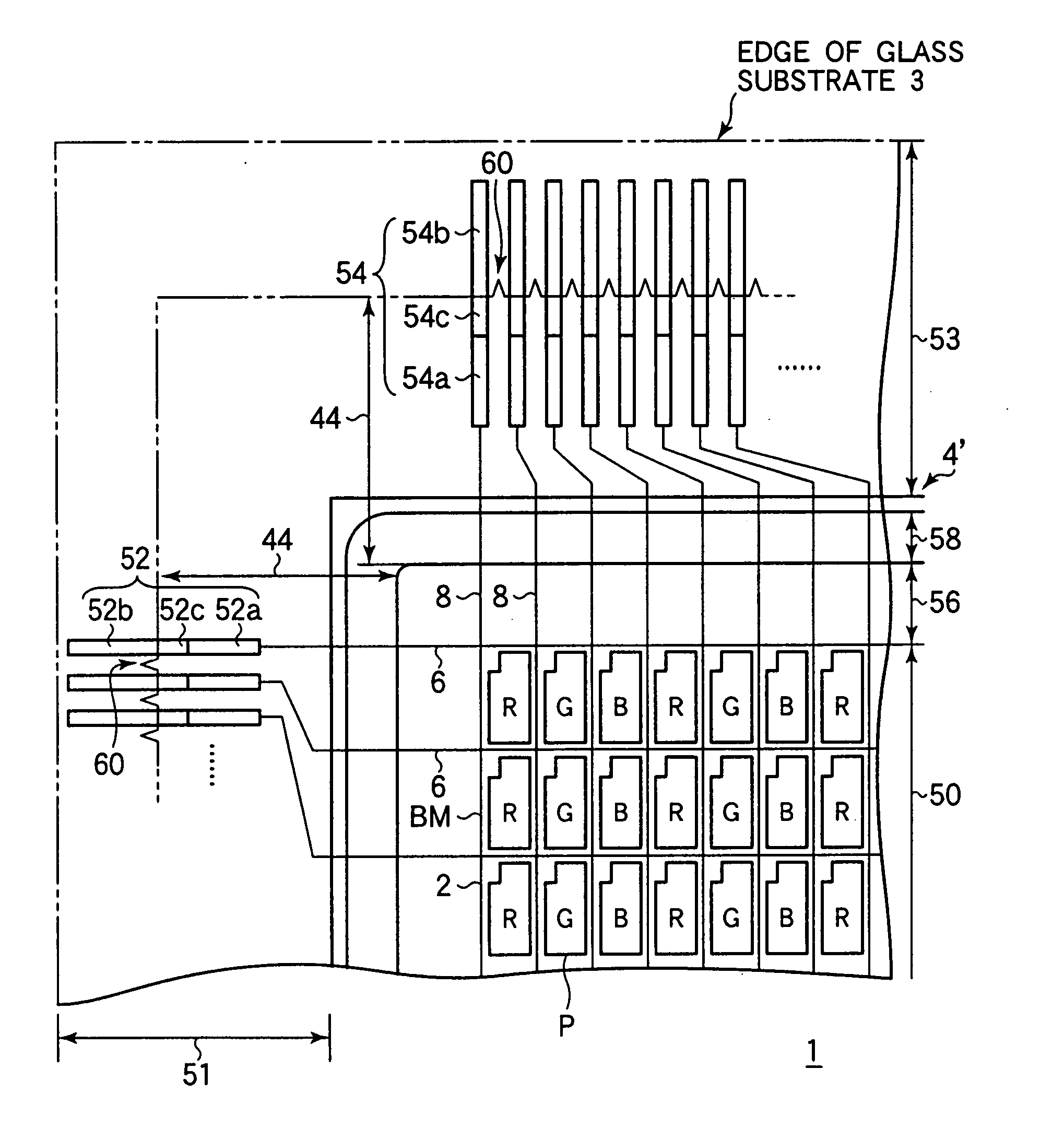
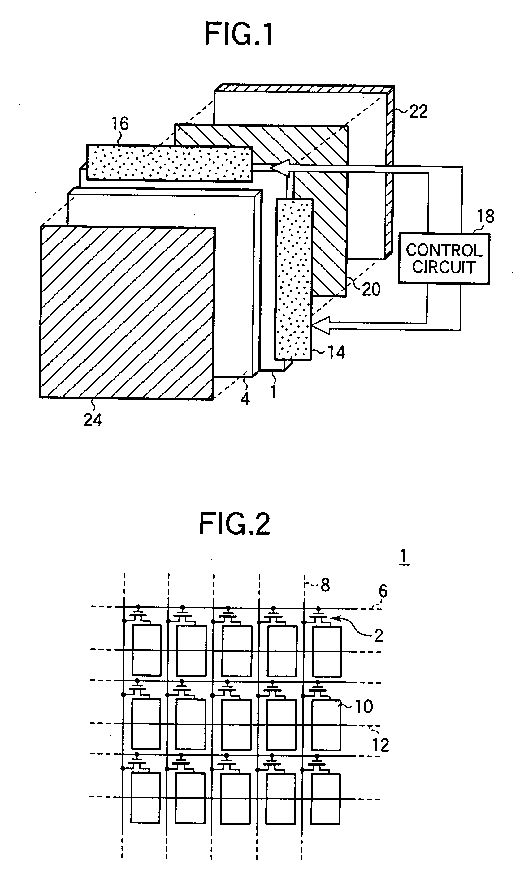
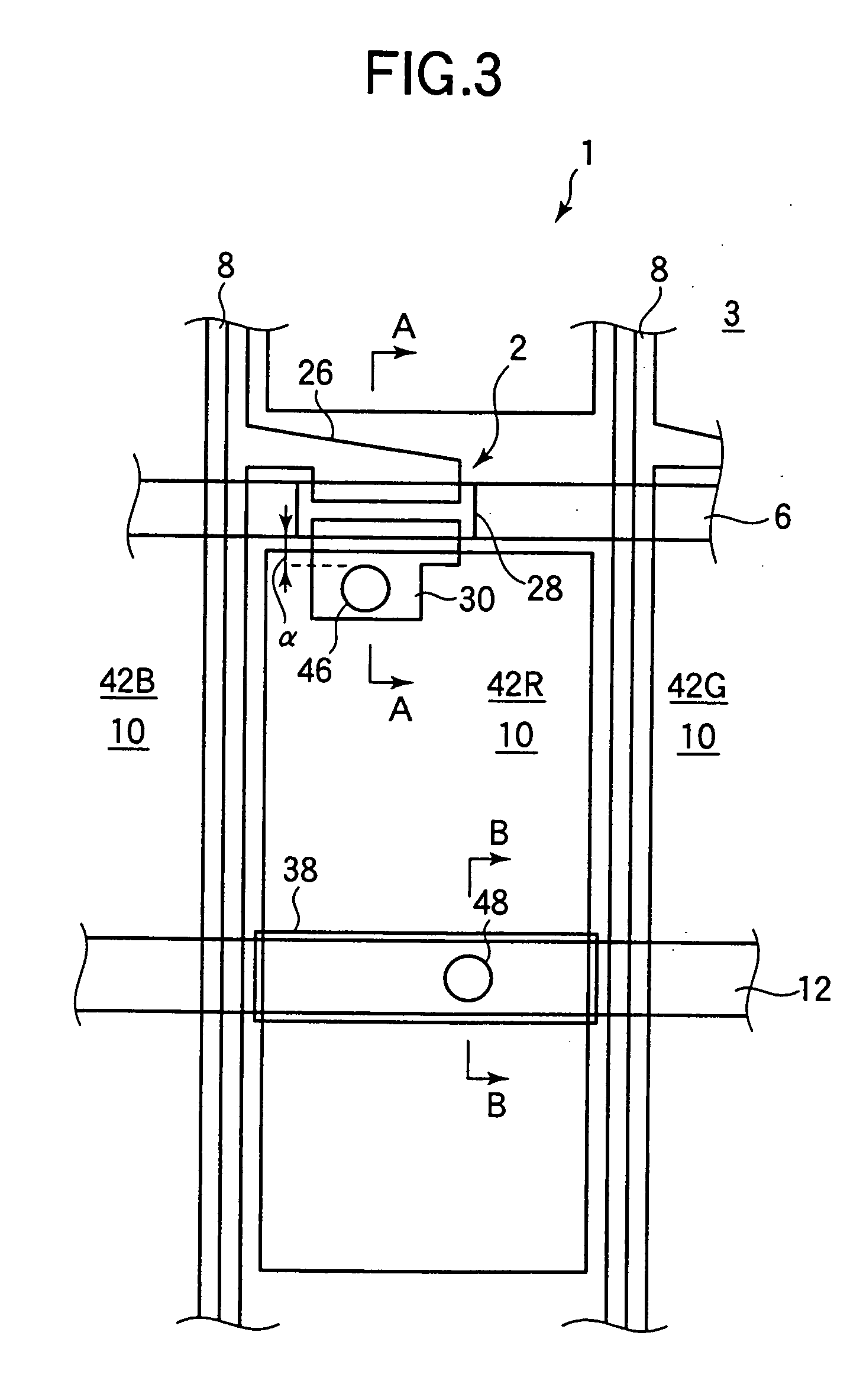
[0096] A substrate for use in a liquid crystal display according to a first embodiment of the present invention, a method of manufacturing the same, and a liquid crystal display using the same will be described with reference to FIGS. 1 to 45 and FIG. 50. First, a rough construction of a liquid crystal display according to this embodiment will be described with reference to FIG. 1. The liquid crystal display according to this embodiment has a construction in which a TFT substrate (array substrate) 1 on which TFTs 2 or the like are formed is made opposite to an opposite substrate 4 on which a common electrode and the like are formed and is bonded thereto, and a liquid crystal is sealed between them. The TFT substrate 1 has a CF-on-TFT structure in which a resin CF layer of, for example, a pigment dispersion type is formed on the side of a formation surface of the TFTs 2, and an OC layer made of an insulating organic resin material is formed on its upper layer.
[0097]FIG. 2 shows an e...
PUM
Property
Measurement
Unit
distance
aaaaa
aaaaa
taper angle
aaaaa
aaaaa
thickness
aaaaa
aaaaa
Abstract
The invention relates to a substrate for use in a liquid crystal display of a CF-on-TFT structure in which a color filter is formed on the side of an array substrate in which a switching element is formed, and has an object to provide a substrate for use in a liquid crystal display, which enables simplification of a manufacturing process typified by a photolithography process and has high reliability. The substrate for use in the liquid crystal display is constructed to include external connection terminals which include first terminal electrodes electrically connected to gate bus lines led out from a plurality of pixel regions arranged on a glass substrate in a matrix form, second terminal electrodes formed of forming material of a pixel electrode and directly on the glass substrate, and electrodecoupling regions for electrically connecting the first and the second terminal electrodes, and which electrically connect an external circuit and the gate bus lines.
Description
[0001] This is a divisional of application Ser. No. 10 / 259,977, filed Sep. 27, 2002.BACKGROUND OF THE INVENTION [0002] 1. Field of the Invention [0003] The present invention relates to a substrate for use in a liquid crystal display, a method of manufacturing the same, and a liquid crystal display using the same, and particularly to a substrate for use in a liquid crystal display, which is used for an active matrix type liquid crystal display using a switching element of a thin film transistor (TFT) or the like, and a method of manufacturing the same. Further, the invention relates to a substrate for use in a liquid crystal display of a CF-on-TFT structure in which a color filter (CF) is formed on the side of an array substrate on which a switching element is formed, a method of manufacturing the same, and a liquid crystal display using the same. [0004] 2. Description of the Related Art [0005] An active matrix type liquid crystal display (LCD) using a TFT as a switching element is d...
Claims
Application Information
Patent Timeline
Application Date:The date an application was filed.
Publication Date:The date a patent or application was officially published.
First Publication Date:The earliest publication date of a patent with the same application number.
Issue Date:Publication date of the patent grant document.
PCT Entry Date:The Entry date of PCT National Phase.
Estimated Expiry Date:The statutory expiry date of a patent right according to the Patent Law, and it is the longest term of protection that the patent right can achieve without the termination of the patent right due to other reasons(Term extension factor has been taken into account ).
Invalid Date:Actual expiry date is based on effective date or publication date of legal transaction data of invalid patent.
Patent Type & AuthorityApplications(United States)

