Supercharge Your Innovation With Domain-Expert AI Agents!

Thin film transistor and method for manufacturing the same

a technology of thin film transistor and manufacturing method, which is applied in the direction of transistors, electrical devices, semiconductor devices, etc., can solve the problems of reducing the reliability of gate oxide films, and achieve the effect of reducing gate leakage and high reliability

Inactive Publication Date: 2006-06-15
DONGBU ELECTRONICS CO LTD
View PDF55 Cites 4 Cited by
  • Summary
  • Abstract
  • Description
  • Claims
  • Application Information

AI Technical Summary

Benefits of technology

[0011] The present invention can provide a thin film transistor and method for manufacturing the same in which ion penetration from extended source / drain regions to a gate oxide film and electrical stress occurring to a gate electrode are suppressed, thereby reducing gate leakage and providing a highly reliable transistor.

Problems solved by technology

Accordingly, electrical stress is generated that reduces the reliability of the gate oxide film.

Method used


Image

  • Thin film transistor and method for manufacturing the same
  • Thin film transistor and method for manufacturing the same
  • Thin film transistor and method for manufacturing the same

Examples


Embodiment Construction

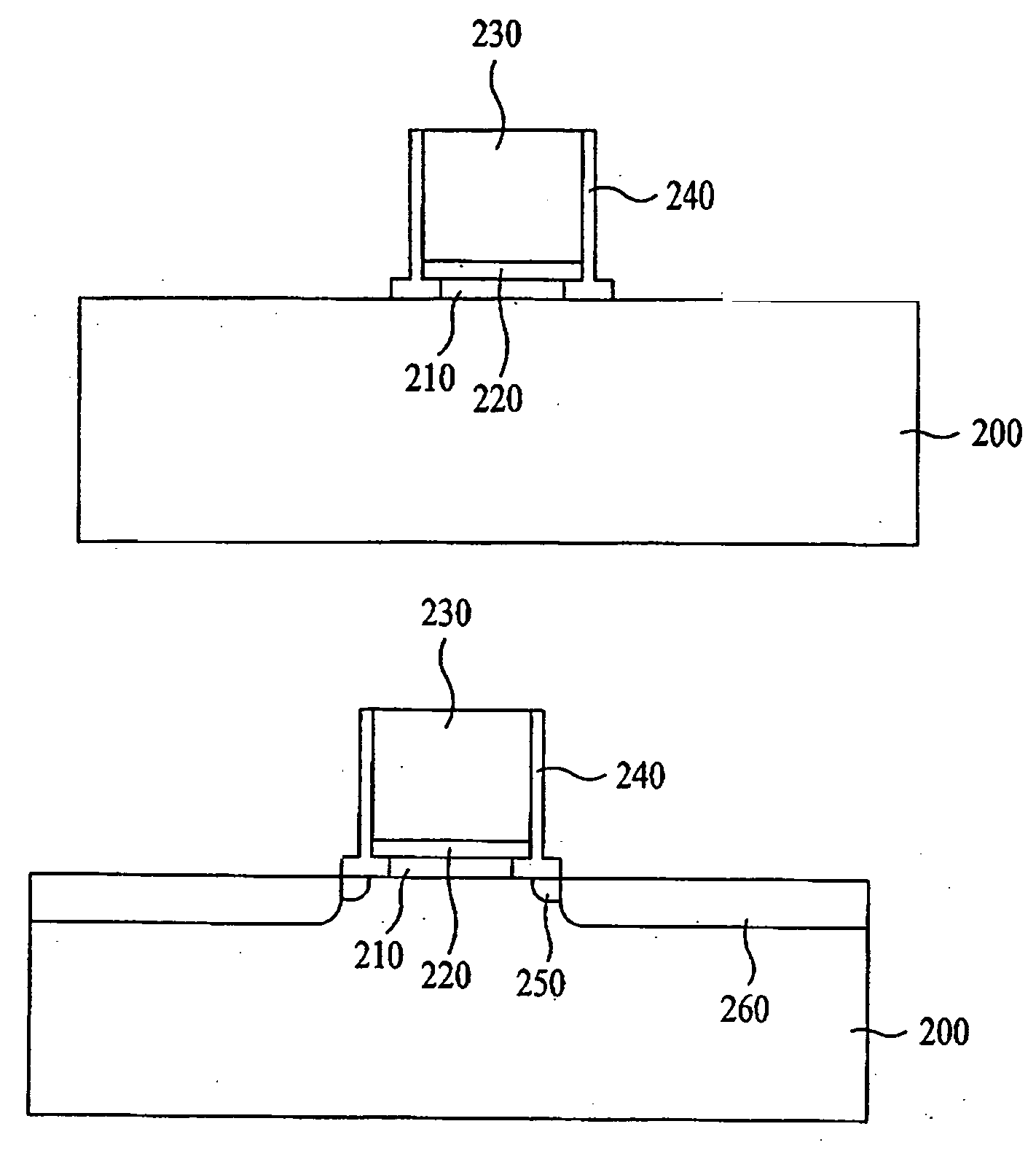
[0019] Reference will now be made in detail to embodiments of the present invention, examples of which are illustrated in the accompanying drawings. Wherever possible, the same reference numbers will be used throughout the drawings to refer to the same or like parts.

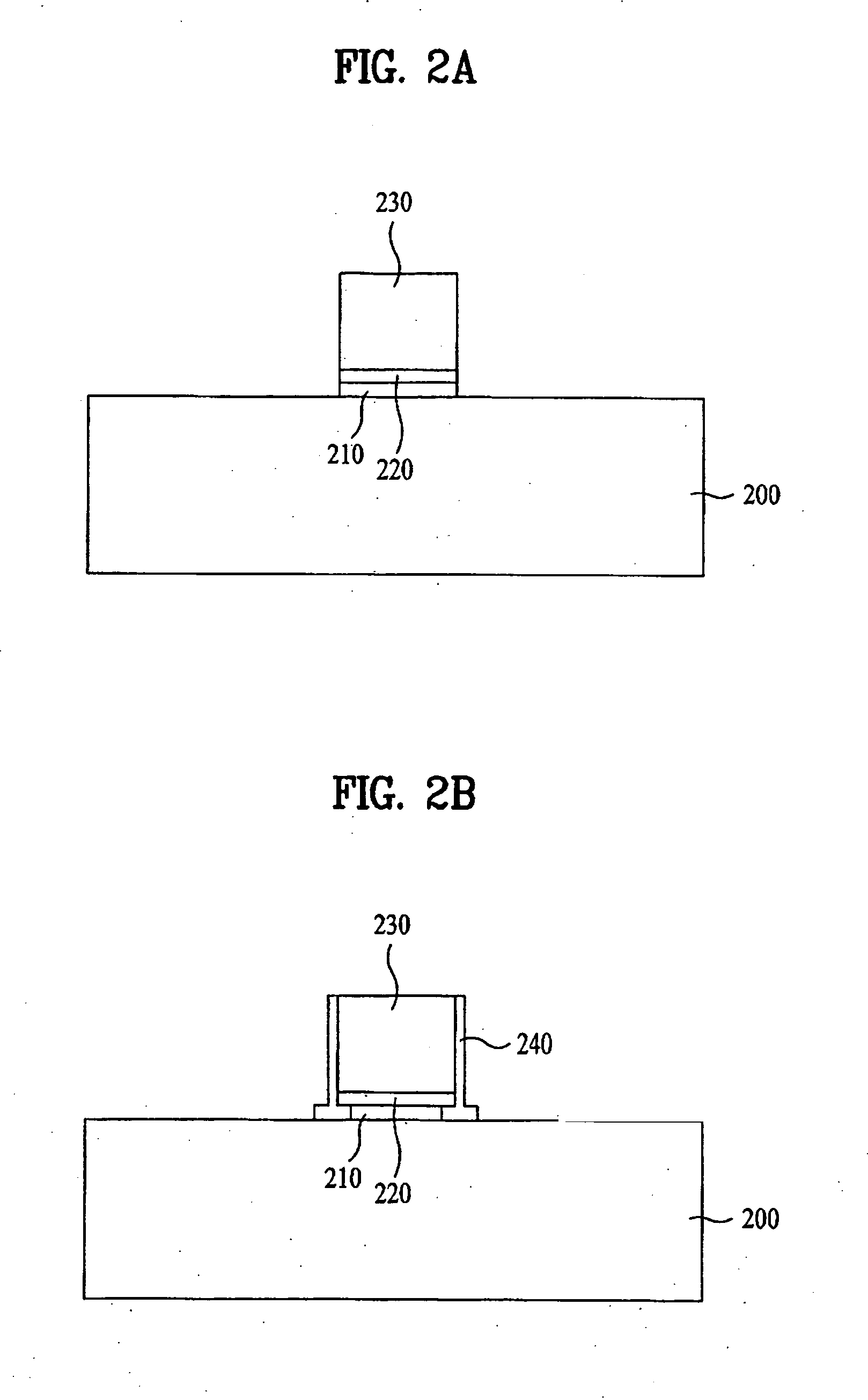
[0020] Referring to FIG. 2A, a gate oxide film 210 is formed on a semiconductor substrate 200, for example, by using a thermal oxidation process. The thermal oxidation process can be performed at a temperature of 650° C. to 750° C. by rapid thermal processing (RTP). The gate oxide film 210 has an exemplary thickness of 100 Å to 300 Å.

[0021] The gate oxide film 210 is then treated with plasma of a high concentration so that a first nitride layer 220 is formed on the top surface of the gate oxide film 210. The first nitride layer 220 has an exemplary thickness of 500 Å to 2000 Å.

[0022] Subsequently, a polysilicon layer 230 is formed on the first nitride layer 220 with a low pressure chemical vapor deposition (LPCVD) pro...


PUM


Abstract

A method for manufacturing a thin film transistor includes forming a gate oxide film on a substrate, forming a first nitride layer on the gate oxide film, forming a polysilicon layer on the first nitride layer, forming a second nitride layer on sidewalls of the gate oxide film, first nitride layer, and polysilicon layer, and implanting impurity ions to form a pocket below the second nitride layer.

Description

CROSS-REFERENCE TO RELATED APPLICATION [0001] This application claims the benefit of Korean Patent Application No. P2004-0106056, filed on Dec. 15, 2004, which is hereby incorporated by reference for all purposes as if fully set forth herein. BACKGROUND OF THE INVENTION [0002] 1. Field of the Invention [0003] The present invention relates to a thin film transistor and method for manufacturing the same, and more particularly, to a thin film transistor and method for manufacturing the same in which ion penetration from source and drain regions is suppressed, and stress generated from gate sidewalls and an interlayer dielectric film is suppressed. [0004] 2. Discussion of the Related Art [0005] The reliability of a complementary metal oxide semiconductor (CMOS) device having high performance and high density is important. If the size of the device is reduced, the thickness of a gate oxide film is correspondingly thinned. However, a power source supplied through a power supplier is not d...

Claims


Application Information

Patent Timeline
IPC IPC(8): H01L21/84H01L21/00
CPCH01L21/26586H01L21/28202H01L29/512H01L29/513H01L29/518H01L29/665H01L29/6656H01L29/6659H01L29/7833H01L29/7842
Inventor PARK, HYUK
Owner DONGBU ELECTRONICS CO LTD
Features
  • R&D
  • Intellectual Property
  • Life Sciences
  • Materials
  • Tech Scout
  • Unparalleled Data Quality
  • Higher Quality Content
  • 60% Fewer Hallucinations
Learn More