

Wired circuit board
a wired circuit board and wire technology, applied in the direction of printed circuit, sustainable manufacturing/processing, printed circuit aspects, etc., can solve the problem of not being able to provide a sufficient heat radiating effect, etc., to improve the heat radiating ability of the wired circuit board and be reliable mounted
- Summary
- Abstract
- Description
- Claims
- Application Information
AI Technical Summary
Benefits of technology
Problems solved by technology
Method used
Image

Examples
example 1
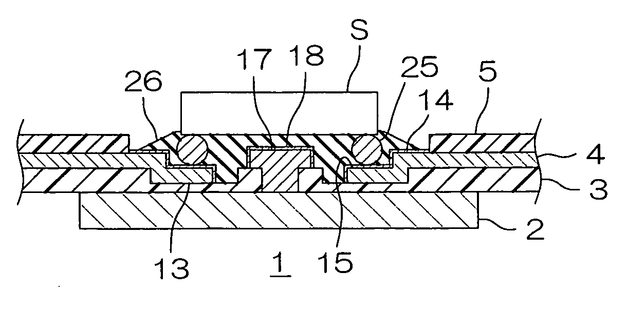
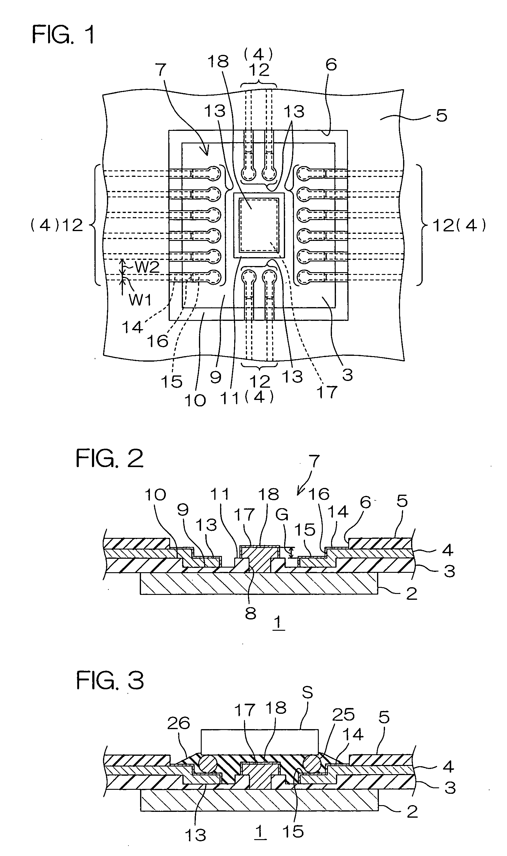
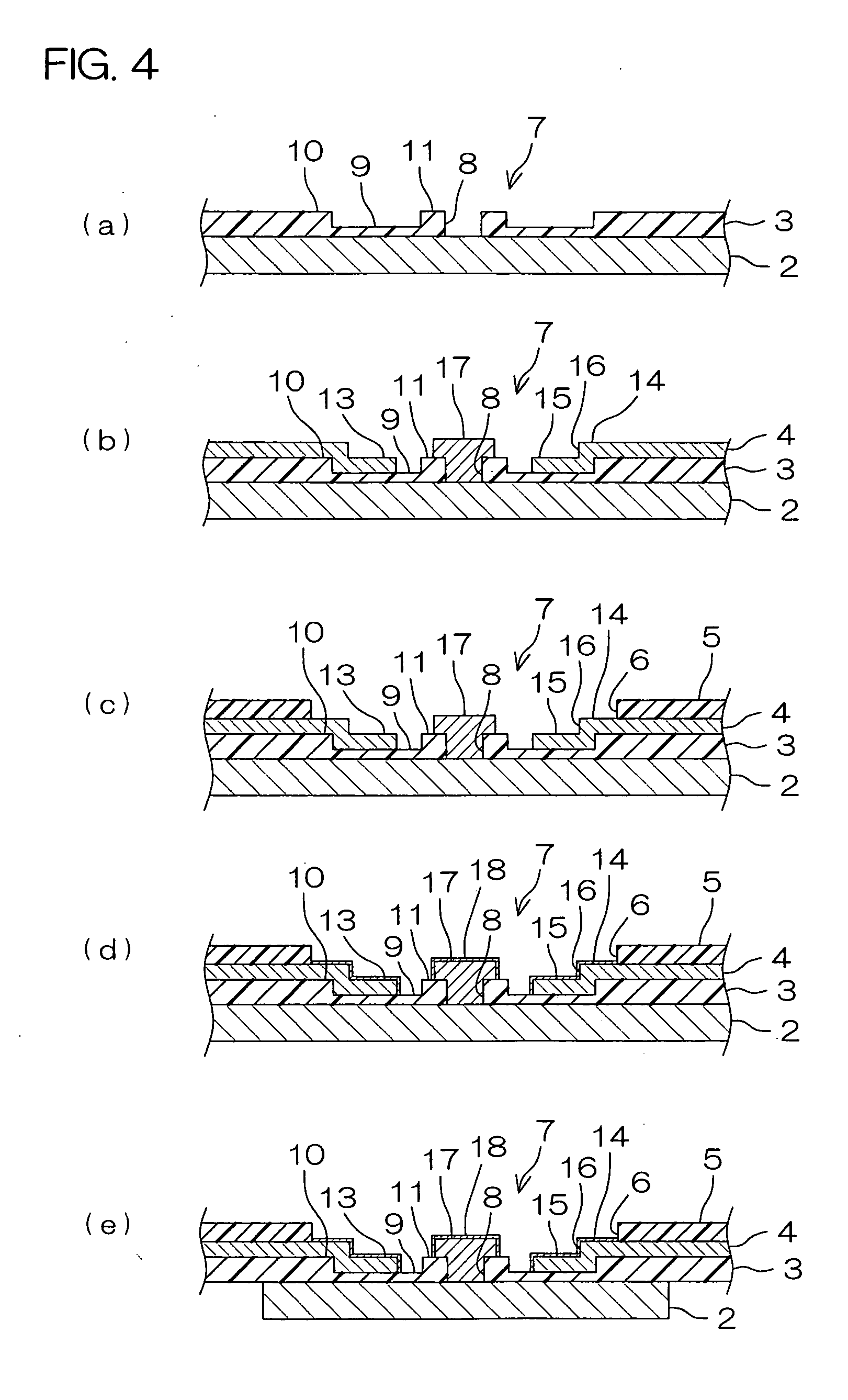
[0096] The stiffer sheet 2 of stainless steel (SUS304) having thickness of 20 μm was prepared (Cf. FIG. 5(a)).
[0097] Then, a solution of precursor of a photosensitive polyimide resin (photosensitive polyamic acid resin) was coated over the entire surface of the stiffener sheet 2. Then, the coated solution was heated for 2 minutes at 120° C., to form the coating 19 of the precursor of the photosensitive polyimide resin (Cf. FIG. 5(b)).
[0098] Thereafter, the photo mask 20 was disposed opposite the coating 19 so that the light shielding portions 20a confronted portions of the coating 19 where the base opening portions 8 were to be formed in the insulating base layer 3 on the stiffener sheet 2; the semi-light-transmitting portions 20b confronted portions of the coating 19 where the thin layer portions 9 of the insulating base layer 3 were to be formed on the stiffener sheet 2; and the total-light-transmitting portions 20c confronted portions of the insulating base layer 3 except the t...
PUM
 Abstract
Description
Claims
Application Information