Power processing interface for passive radio frequency identification system

a technology of radio frequency identification and power processing, which is applied in the direction of frequency-division multiplex, process and machine control, instruments, etc., can solve the problems of unstable system, easy to be affected by noise interference, and the low-pass filter b>13/b> is not able to provide sufficient filtering effect, so as to avoid over-degradation of operating voltage

Inactive Publication Date: 2006-06-22
HOLTEK SEMICON
View PDF6 Cites 28 Cited by
  • Summary
  • Abstract
  • Description
  • Claims
  • Application Information

AI Technical Summary

Benefits of technology

[0013] In accordance with another aspect of the present invention, a power processing interface for the passive RFID is provided. The power processing interface is able to provide an effective minimum operating voltage during the modulation process, so that the over-degradation of the operating voltage can be avoided.
[0014] In accordance with a further aspect of the present invention, a power processing interface for a radio frequency identification system is provided. The power processing interface includes a resonance circuit for inducing a first signal transmitted from a terminal as an AC voltage, a first rectifier circuit electrically connected to the resonance circuit for converting the AC voltage into a DC voltage, a filter circuit electrically connected to the first rectifier circuit for g

Problems solved by technology

However, in the conventional passive RFID system, the tag 02 is not connected to the ground so that it is easily affected by the interference of noise.
In addition, the RC low-pass filter 13 is not able to provide sufficient filtering effect due to the limitations of space and costs for the integrated circuit.
That is, the DC voltage increases as the tag 02 moves toward the reader 01 but decreases a

Method used


Image

  • Power processing interface for passive radio frequency identification system
  • Power processing interface for passive radio frequency identification system
  • Power processing interface for passive radio frequency identification system

Examples


Embodiment Construction

[0044] The present invention will now be described more specifically with reference to the following embodiments. It is to be noted that the following descriptions of preferred embodiments of this invention are presented herein for the purposes of illustration and description only; it is not intended to be exhaustive or to be limited to the precise form disclosed.

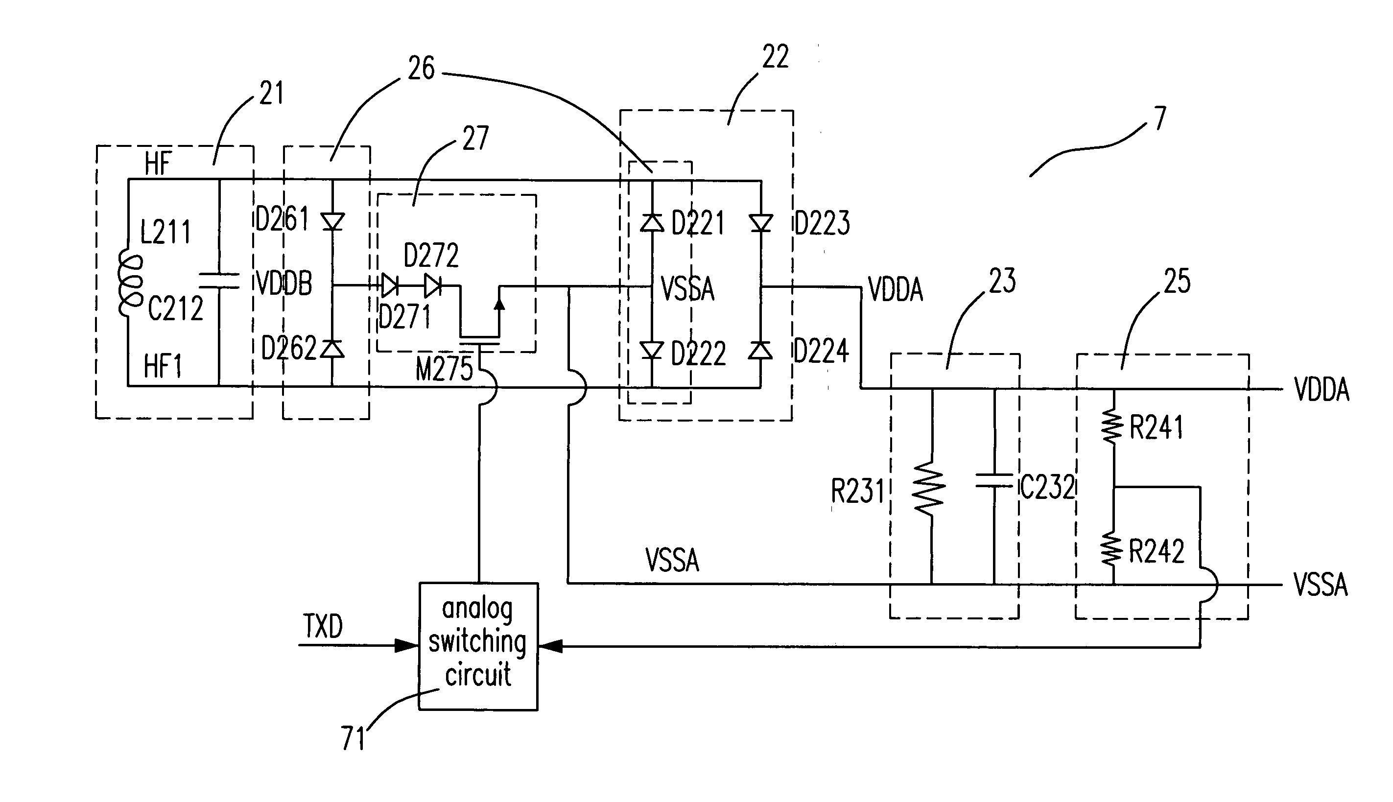
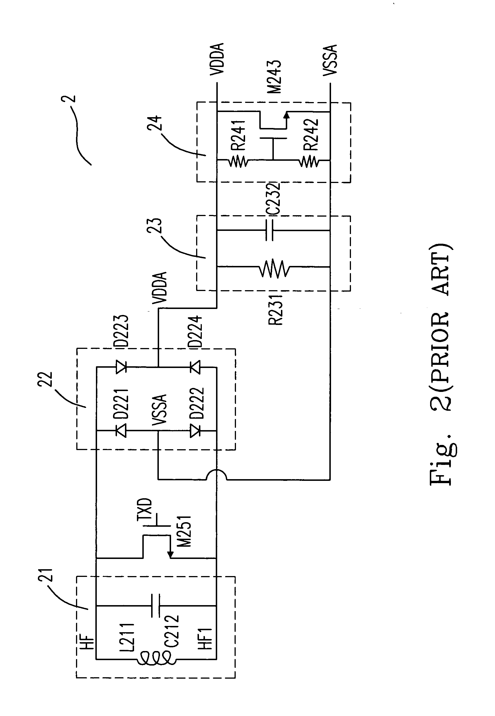
[0045] The present invention provides a stable operating voltage for the tag of the passive RFID system during the data modulation and demodulation processes. In the conventional tag structure shown in FIG. 4, the voltage limiter 24 includes two resistors R241 and R242 and a transistor M243. The two resistors R241 and R242 are used as the voltage detecting components for over-voltage detection, and the transistor M243 is used as the voltage-limiting limited component for voltage limitation. In the present invention, the position of the voltage detecting components R241 and R242 remains the same to detect the operating volt...


PUM


Abstract

A power processing interface for a radio frequency identification system is provided. The power processing interface includes a resonance circuit for inducing a first signal transmitted from a terminal as an AC voltage, a first rectifier circuit electrically connected to the resonance circuit for converting the AC voltage into a DC voltage, a filter circuit electrically connected to the first rectifier circuit for generating an operating voltage in response to the DC voltage, a voltage-detecting circuit electrically connected to the filter circuit and the first rectifier circuit for detecting the magnitude of the operating voltage, a second rectifier circuit electrically connected to the resonance circuit, and a voltage-clamping modulation circuit electrically connected to the first rectifier circuit, the voltage-detecting circuit and the second rectifier circuit for controlling the conduction of the second rectifier circuit in response to the output of the voltage-detecting circuit so as to bypass the excessive current, and for providing a minimum voltage to the radio frequency identification system during the modulation process so as to keep the radio frequency identification system in a normal operation.

Description

FIELD OF THE INVENTION [0001] The present invention relates to a power processing interface, and more particularly to a power processing interface for the passive radio frequency identification (RFID) system. BACKGROUND OF THE INVENTION [0002] Please refer to FIG. 1, which shows the structure of the passive RFID system in the prior art. The electromagnetic induction is proceeded through the inductors L101 and L111 respectively implicit in the reader 01 and the tag 02, so that the energy and information can be transmitted therebetween for being identified. The inductor L101 is implicit in the resonance circuit 10 of the reader 01, and the inductor L111 is implicit in the resonance circuit 11 of the tag 02. The fixed radio frequency carrier signal emitted from the inductor L101 of the reader 01 is induced by the inductor L111 of the tag 02 and then serves as an AC power source. After that, the AC power source is converted into a DC voltage via the bridge rectifier circuit 12, which ma...

Claims


Application Information

Patent Timeline
IPC IPC(8): G06K19/06
CPCG06K19/0701G06K19/0723
Inventor WANG, MINKUNSHEN, CHUN-LINHSU, CHI-HOCHEN, CHI-BING
Owner HOLTEK SEMICON
Why Eureka
Try Eureka