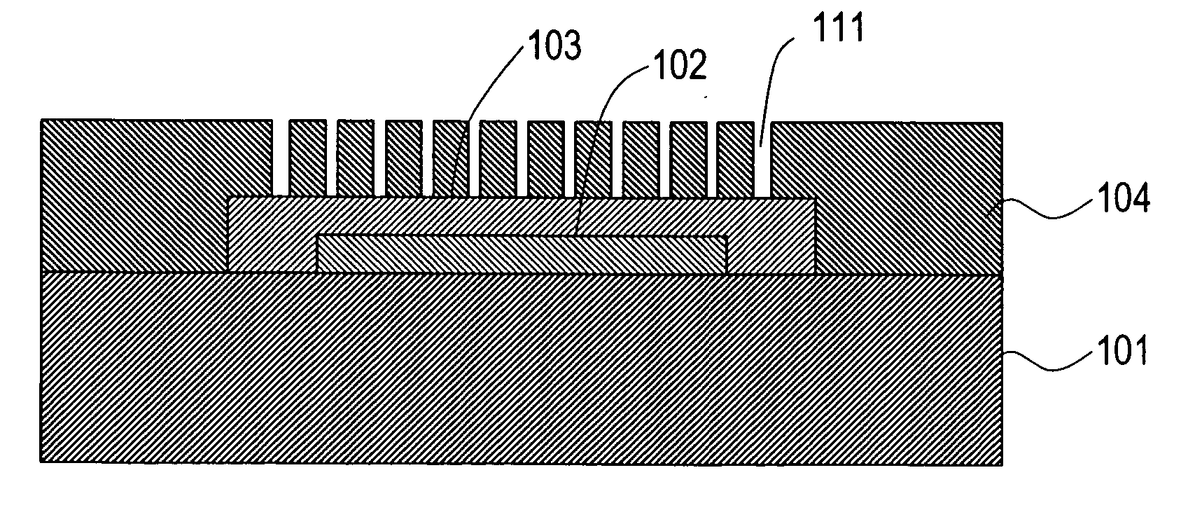
Method for fabricating the same
a technology of electronic devices and methods, applied in the field of electronic devices, can solve the problems of insufficient sensitivity, difficult to completely exhaust remaining sihsub>4 /sub>and hsub>2 /sub>gases, and inability to expect the effect of increasing the degree of vacuum significantly
- Summary
- Abstract
- Description
- Claims
- Application Information
AI Technical Summary
Benefits of technology
Problems solved by technology
Method used
Image
Examples
embodiment 1
[0134] Hereinafter, a first preferred embodiment of the present invention will be described with reference to the accompanying drawings.
[0135] An electronic device according to this preferred embodiment is an image sensor including an infrared sensing element and a visible light detecting element that are integrated together on the same substrate. An exemplary configuration for such an image sensor including an infrared sensing element and a visible light detecting element is disclosed in Japanese Patent Application Laid-Open Publication No. 2003-17672, for example.
[0136] By arranging both the infrared sensing element and visible light detecting element on the same substrate by a semiconductor process, the manufacturing cost and the device size can be both reduced. If an infrared image sensor and a visible light image sensor are separately provided on two different substrates, then optical alignment needs to be carried out accurately after that and the misalignment between the inf...
embodiment 2
[0193] Hereinafter, a second preferred embodiment of the present invention will be described.
[0194]FIG. 24 illustrates a preferred embodiment in which a gettering thin film is provided inside the micro vacuum package (i.e., within the cavity 163′). The gettering thin film is activated under the heat generated by the microheater portion 173 and can adsorb the gas that is present inside the micro vacuum package (i.e., within the cavity 163′) and decrease its pressure.
[0195] In this preferred embodiment, a gettering thin film 185 is provided under the microheater portion 173 and under the silicon dioxide film that functions as an etch stop layer. This gettering thin film 185 may have a thickness of 500 nm, for example. To keep the degree of vacuum inside the micro vacuum package high by utilizing the gettering thin film 185, the gettering thin film 185 needs to have a sufficient thickness. And its preferred thickness depends on the internal volume of the micro vacuum package.
[0196] ...
embodiment 3
[0215] Hereinafter, a third preferred embodiment of the present invention will be described with reference to FIG. 26, which illustrates the cross-sectional structure of a micro vacuum package in an electronic device according to this preferred embodiment. A great number of cavities are actually made on a single substrate but just one of them is illustrated as a typical one in FIG. 26 for the sake of simplicity.
[0216] The micro vacuum package illustrated includes a cap member 20 to close a recess on a silicon substrate 160. In this preferred embodiment, the cap member 20 is made of silicon (with a thickness of 1 μm to 1,000 μm).
[0217] If the thickness of a gettering thin film 185 exceeded 100 μm, then it would take more than 10 hours to form the thin film, which would cause a significant decline in productivity. In addition, the film would have increased stress and the chances of film peeling would be stronger. If the thickness of the gettering thin film 185 is limited to 10 μm or...
PUM
 Abstract
Description
Claims
Application Information
 - Generate Ideas
- Intellectual Property
- Life Sciences
- Materials
- Tech Scout
- Unparalleled Data Quality
- Higher Quality Content
- 60% Fewer Hallucinations
Browse by: Latest US Patents, China's latest patents, Technical Efficacy Thesaurus, Application Domain, Technology Topic, Popular Technical Reports.
© 2025 PatSnap. All rights reserved.Legal|Privacy policy|Modern Slavery Act Transparency Statement|Sitemap|About US| Contact US: help@patsnap.com


