Eureka AIR delivers breakthrough ideas for toughest innovation challenges, trusted by R&D personnel around the world.

CMOS image sensor and method for fabricating the same

a technology of image sensor and manufacturing method, which is applied in the field of image sensor, can solve the problems of complex fabrication process requiring multi-phase photo-processing, complicated driving method, and high power consumption, and achieve excellent transmissivity and improve the light-receiving efficiency of image sensor

Inactive Publication Date: 2006-06-22
DONGBU ELECTRONICS CO LTD
View PDF7 Cites 14 Cited by
  • Summary
  • Abstract
  • Description
  • Claims
  • Application Information

AI Technical Summary

Benefits of technology

[0012] An advantage of the present invention is to provide a CMOS image sensor and a method for fabricating the same, to improve the light-receiving efficiency of the image sensor by forming a microlens of a polymer exhibiting excellent transmissivity.

Problems solved by technology

Charge-coupled devices, have the disadvantages of complicated driving method, high power consumption, and complicated fabrication processes requiring multi-phased photo-processes.
Additionally, integration of complementary circuitry such as a control circuit, a signal processor, and an analog-to-digital converter into a single-chip charge coupled device is difficult, thereby hindering development of compact-sized products using such image sensors.
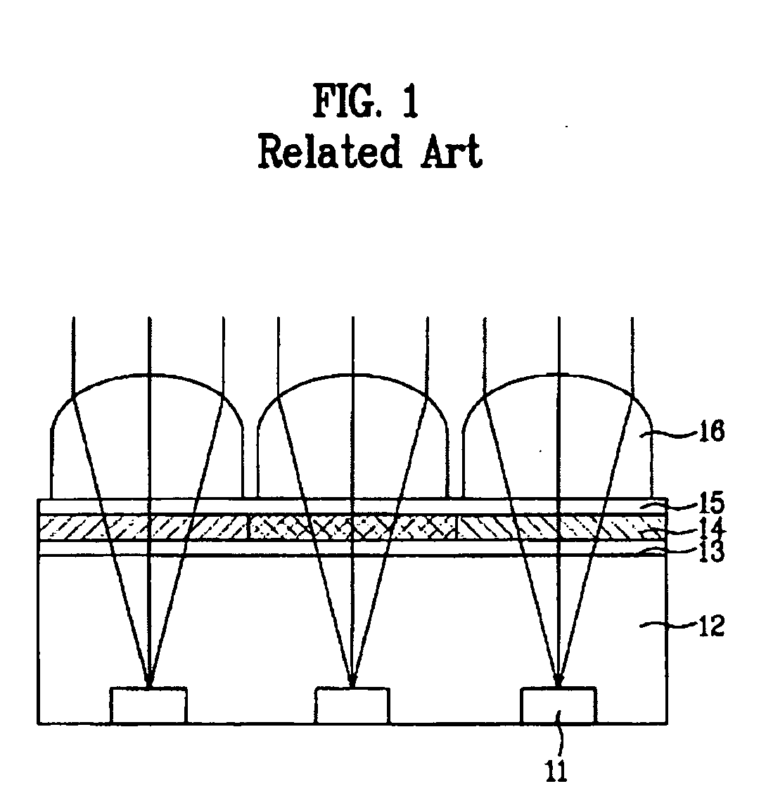
Use of photoresist material for microlenses 16, however, exhibits poor light transmissivity characteristics and thus limits the light-receiving efficiency of an CMOS image sensor and consequently it also limits any further improvement of this critical characteristic.

Method used


Image

  • CMOS image sensor and method for fabricating the same
  • CMOS image sensor and method for fabricating the same
  • CMOS image sensor and method for fabricating the same

Examples


Embodiment Construction

[0023] Reference will now be made in detail to exemplary embodiments of the present invention, examples of which are illustrated in the accompanying drawings. Wherever possible, like reference numbers will be used throughout the drawings to refer to the same or similar parts.

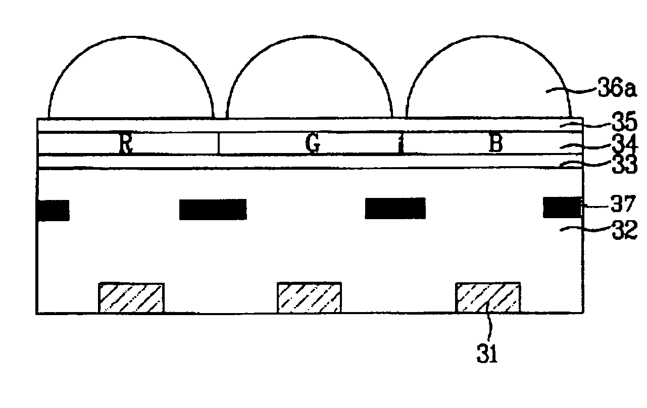
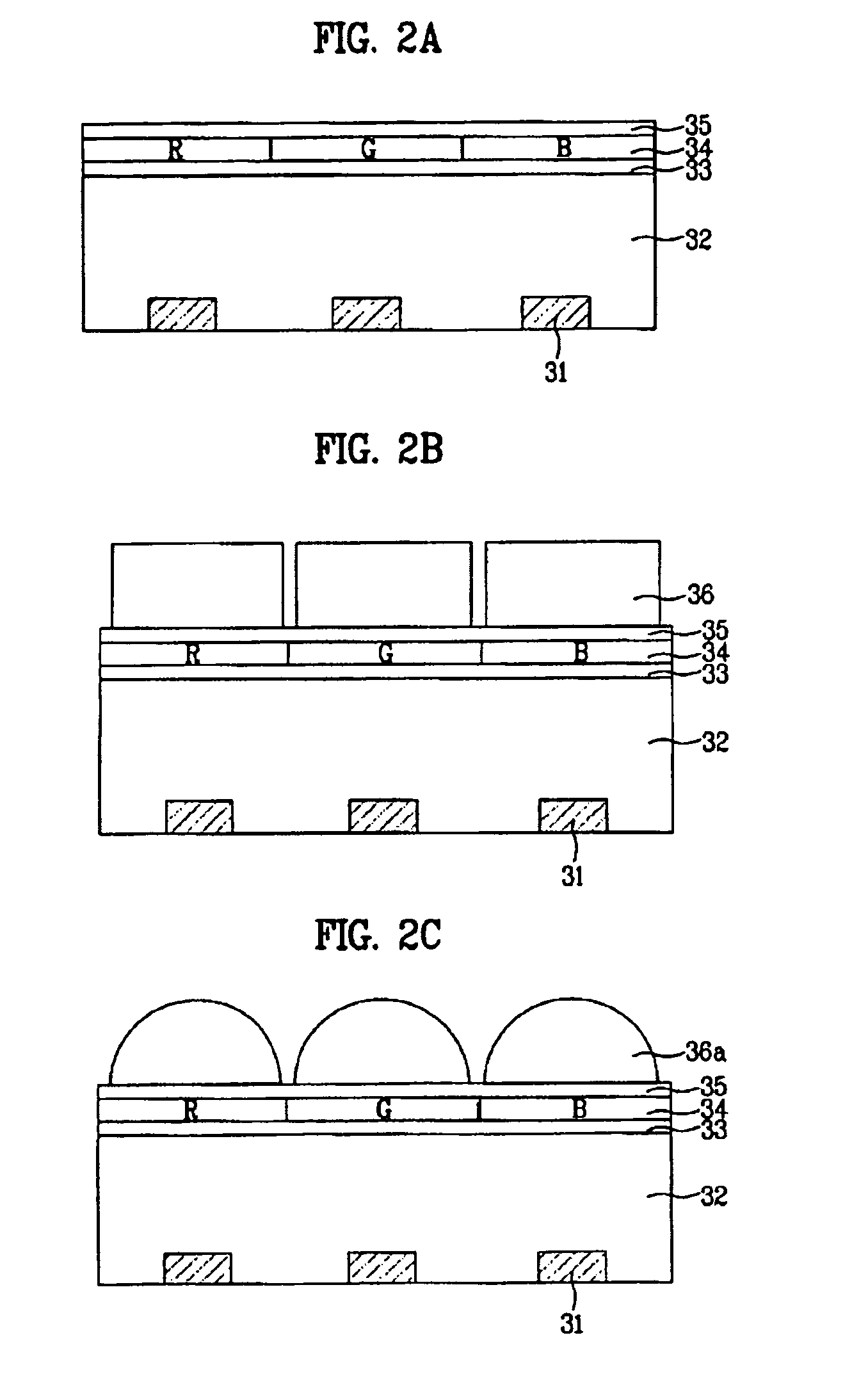
[0024]FIGS. 2A-2C illustrate a process for fabricating a CMOS image sensor according to an embodiment of the present invention.

[0025] Referring to FIG. 2A, at least one photodiode 31 for generating electrical charges according to the amount of incident light is disposed on a semiconductor substrate (not shown). In one embodiment, three such photodiodes per pixel unit of a color CMOS image sensor are arranged at fixed intervals. An insulating interlayer 32 is formed atop the photodiodes 31 to be in contact with surfaces of the semiconductor substrate and to completely cover the photodiodes. The insulating interlayer 32 may be formed as a multi-layered structure to include an optical-shielding layer (not shown),...


PUM


Abstract

A CMOS image sensor and a method for fabricating the same with improved light-receiving efficiency of the active device, e.g., a photodiode. The CMOS image sensor includes at least one photodiode positioned on a semiconductor substrate; and a microlens disposed above each photodiode, wherein the microlens is formed of a polymer exhibiting excellent transmissivity.

Description

CROSS-REFERENCE TO RELATED APPLICATIONS [0001] This application claims the benefit of Korean Application No. 10-2004-0109602 filed on Dec. 21, 2004, which is hereby incorporated by reference for all purposes as if fully set forth herein. BACKGROUND OF THE INVENTION [0002] 1. Field of the Invention [0003] The present invention relates to image sensors, and more particularly, to a CMOS image sensor having improved light-receiving efficiency and a method for fabricating the same. [0004] 2. Discussion of the Related Art [0005] Image sensors are semiconductor devices for converting an optical image into an electrical signal and include charge-coupled devices and complementary metal-oxide-semiconductor (CMOS) image sensors. [0006] A general charge-coupled device includes an array of photodiodes converting light signals into electrical signals, a plurality of vertical charge-coupled devices formed between each vertical photodiode aligned in a matrix-type configuration and vertically transm...

Claims


Application Information

Patent Timeline
Patent Type & Authority Applications(United States)
IPC IPC(8): H01L33/00
CPCH01L27/14621H01L27/14627H01L27/14685H01L27/146H01L31/10
Inventor KOH, KWAN JU
Owner DONGBU ELECTRONICS CO LTD
Why Eureka
Eureka Blog
Learn More