Check patentability & draft patents in minutes with Patsnap Eureka AI!

Method for producing a microlens array

Inactive Publication Date: 2006-06-22
EASTMAN KODAK CO
View PDF7 Cites 10 Cited by
  • Summary
  • Abstract
  • Description
  • Claims
  • Application Information

AI Technical Summary

Benefits of technology

[0008] The present invention relates to an improved method of forming microlens arrays on electronic image sensors. The improvement involves a method whereby adjacent microlenses can be packed close enough together to eliminate any significant gaps between them while allowing the use of a preferred spherical shape. The method involves the use of a template with the desired relief image for the microlens array. The imprint stamp is brought into contact with a polymerizable fluid composition such that the relief image is completely filled with said polymerizable fluid composition. The fluid nature of the polymerizable composition and capillary action allows this relief image filling to be accomplished with very little pressure. The imprint stamp is made of a material that is transparent to the wavelengths of light necessary to photochemically harden the polymerizable fluid composition. This allows irradiation through the imprint stamp while it is in contact with the polymerizable fluid composition. The result of this irradiation is a hardening of the polymerizable fluid composition. This hardening permits subsequent removal of the imprint stamp while the hardened polymerizable composition retains the desired microlens shape. The hardened polymerizable composition has the necessary optical transmission and stability properties that allow it to be used directly as the microlens array on electronic image sensors without having to transfer the microlens shape into an underlying layer by etching techniques.

Problems solved by technology

If they were to touch the patterns would flow together and not produce the desired microlens shape.
Thus, this technique always results in gaps between adjacent microlenses.
Judicious adjustment of the etch rates can result in smaller gaps in the final microlens array.
Although this method does result in reduced gaps, there isn't enough process latitude to completely eliminate the gaps around the entire perimeter of the pixel.
Other disadvantages of this method include the need for the extra pattern transfer RIE step and the risk of damage to the underlying image sensor from the plasma environment.
The range of densities results in a range of solubilities of the exposed photoresist film.
First, as should be obvious, the design and production of the mask is quite complicated and expensive.
These types of photoresists are difficult to find since most photoresist development work has been aimed at the high contrast needed to produce the high-density circuits used in modern electronic devices.
Also, these photoresists most likely do not contain the characteristics necessary for use as the final microlens material.
These distortions are not of significant size to effect the quality of fiber optic or display devices however the pixel sizes are much smaller for image sensors and such distortions would severely effect performance.

Method used


Image

  • Method for producing a microlens array
  • Method for producing a microlens array
  • Method for producing a microlens array

Examples


Embodiment Construction

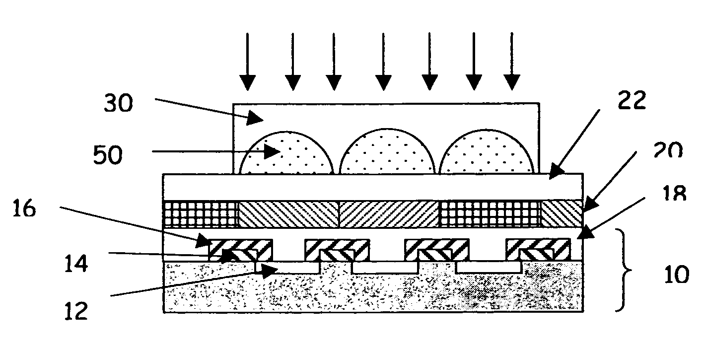
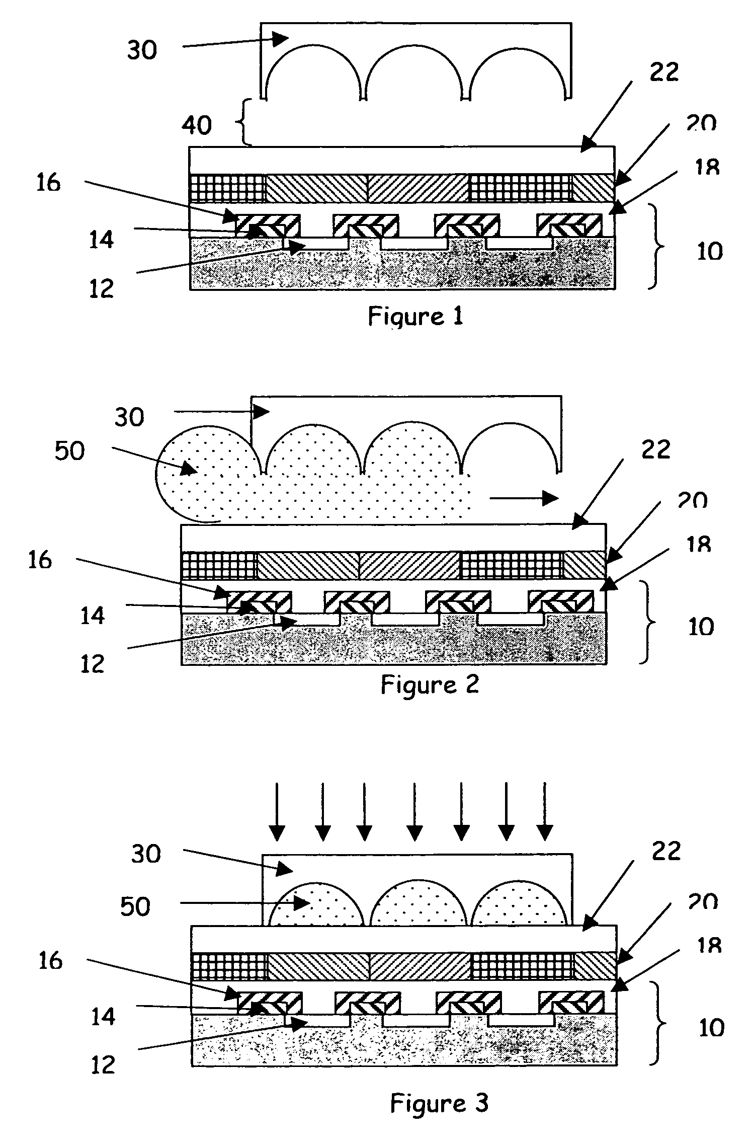
[0015] In a preferred embodiment of the present invention, illustrated in FIGS. 1-5, a method is provided by which a microlens array is formed on electronic image sensors. The method provides for adjacent microlenses packed close enough together to eliminate any significant gaps between them while allowing the use of a preferred spherical shape.

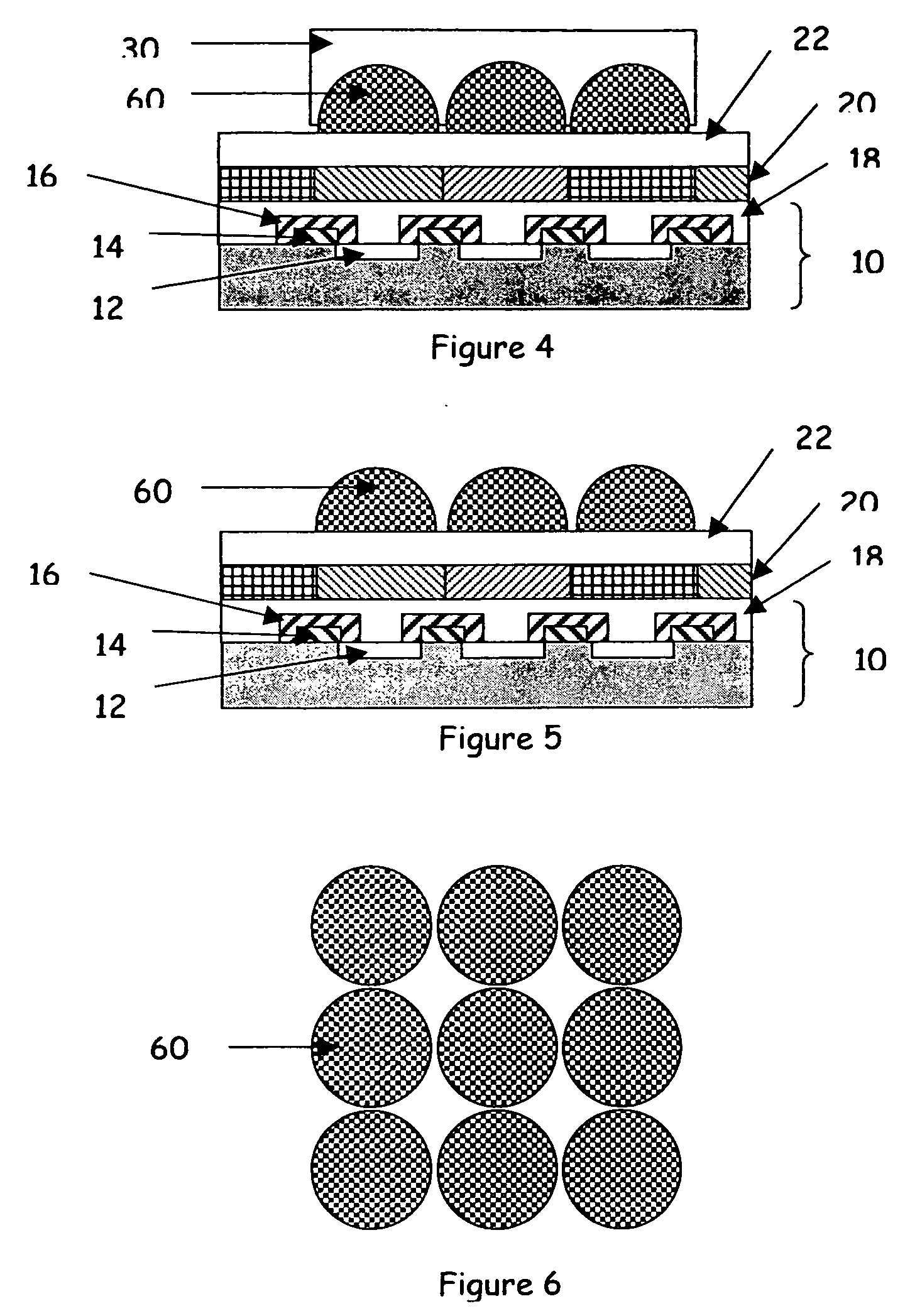
[0016] Referring to FIG. 1, a semiconductor portion 10, comprising photoactive areas 12, electrodes 14, and lightshields 16 is shown as representative of the typical elements of the semiconductor portion of a solid state electronic image sensor. For most applications of electronic image sensors, it is desirable to enhance the characteristics of the incoming electromagnetic radiation. In order to facilitate this enhancement, a planarization layer 18 is often applied to the surface of the semiconductor portion of the electronic image sensor. This planarization layer 18 can consist of a variety of materials the only requirements being that it d...


PUM

PropertyMeasurementUnit
Transparencyaaaaaaaaaa
Wavelengthaaaaaaaaaa

Abstract

A method for creating microlenses, the method includes the steps of providing a substrate having a plurality of photoactive areas; providing a photopolymerizable fluid composition on the substrate; providing a template which is transparent to photoactive wavelengths and which includes a plurality of curved surfaces that act to focus incident light onto the photoactive area; placing the template on the photopolymerizable fluid composition which causes the fluid material to spread and substantially fill the curved surfaces of the template; and irradiating light through the template and onto the photopolymerizable fluid composition for hardening photopolymerizable fluid composition into microlenses spanning the substrate.

Description

FIELD OF THE INVENTION [0001] This invention relates to the fabrication of microlens arrays on the surface of electronic image sensors. BACKGROUND OF THE INVENTION [0002] There continues to be a push to produce ever-higher resolution in electronic image sensors. This means the surface area of individual pixels is becoming smaller and thus the amount of light impinging on each pixel is also decreasing. Advances in the technology of the underlying electronic image sensor have helped boost the signal-to-noise ratio to compensate for the decreasing amount of light. However, since the photoactive part of a pixel is often only 50% or less of the total pixel area, the fabrication of microlens arrays aligned to the pixel arrays has proven to be a very effective way of increasing the fraction of incident light striking the photoactive area of the pixels. [0003] A very efficient and manufacturable method of producing microlens arrays has been to form patterns in photoresist materials by stand...

Claims


Application Information

Patent Timeline
IPC IPC(8): B29D11/00
CPCB29C43/021B29C43/18B29D11/00365B29L2011/0016G02B3/0012G02B3/0056H01L27/14627H01L27/14685
Inventor WAKE, RONALD W.
Owner EASTMAN KODAK CO
Features
  • R&D
  • Intellectual Property
  • Life Sciences
  • Materials
  • Tech Scout
  • Unparalleled Data Quality
  • Higher Quality Content
  • 60% Fewer Hallucinations
Learn More