
Semiconductor device and voltage-controlled oscillation circuit

a technology of oscillation circuit and oscillation frequency, which is applied in the direction of pulse generator, pulse manipulation, pulse technique, etc., can solve the problem of limited duty ratio of generated clock signal, limited range of internal generator clock signal oscillation frequency, and limited range of reference clock signal usable in dll circuit, etc. problem, to achieve the effect of high accuracy and more delicate control of delay tim

Active Publication Date: 2006-06-22
SOCIONEXT INC
View PDF5 Cites 11 Cited by
  • Summary
  • Abstract
  • Description
  • Claims
  • Application Information

AI Technical Summary

Benefits of technology

[0016] According to the present invention, the internal oscillation circuits whose oscillation frequencies are controllable according to the result of the comparison in the phase comparing circuit are provided independently from one another, and the output of one of the internal oscillation circuits can be outputted as the feedback clock signal. This makes it possible to output the feedback clock signal keeping a proper duty ratio even when the operation speed is high, allowing arbitrary adjustment of the delay time before the inputted signal is outputted. Further, since the plural internal oscillation circuits with different oscillation frequencies are provided, reference clock signals with various frequencies are usable.
[0017] Each of the internal oscillation circuits may include a load capacitance circuit which is connected to output ends of logic gates with inverted outputs included in the internal oscillation circuit and whose load capacitance value is variable according to a control signal by utilizing oxide film capacitance of a MOS transistor as load capacitance. Providing the load capacitance circuit enables more delicate control of the delay time, allowing high-accuracy adjustment of the delay time.
[0018] Further, the voltage-controlled oscillation circuit of the present invention includes: a plurality of independent internal oscillation circuits with different oscillation frequencies; and a selecting circuit, wherein the oscillation frequencies of the internal oscillation circuits are controlled according to a voltage of an externally supplied voltage signal, and the selecting circuit selectively outputs an output of one of the internal oscillation circuits according to a selection signal relating to selection of the output. This makes it possible to output a clock signal with an arbitrary frequency keeping a proper duty ratio even when the operating rate is high.

Problems solved by technology

However, a semiconductor device such as the DLL circuit generally has only one voltage-controlled oscillation circuit.
Therefore, a range of the oscillation frequency of the clock signal internally generatable has been conventionally limited, and a range of the reference clock signal usable in the DLL circuit has been also limited.
This has posed a problem that a duty ratio of the generated clock signal, which should be 5:5 as shown in FIG. 9A and FIG. 9B, may possibly become improper as shown in FIG. 9C and FIG. 9D.
The improper duty ratio of the generated clock signal may possibly cause a great trouble under a high-speed operation as shown especially in FIG. 9D.
If it is used in, for example, the DLL circuit, the adjustment of the delay time may possibly become unfeasible under the high-speed operation.
Since the bulk capacitors Ca, Cb are basically large in capacitance as described above, the control of a small oscillation frequency, namely, delicate adjustment of the delay time is not feasible.

Method used


Image

  • Semiconductor device and voltage-controlled oscillation circuit
  • Semiconductor device and voltage-controlled oscillation circuit
  • Semiconductor device and voltage-controlled oscillation circuit

Examples


Embodiment Construction

[0031] Hereinafter, embodiments of the present invention will be described based on the drawings.

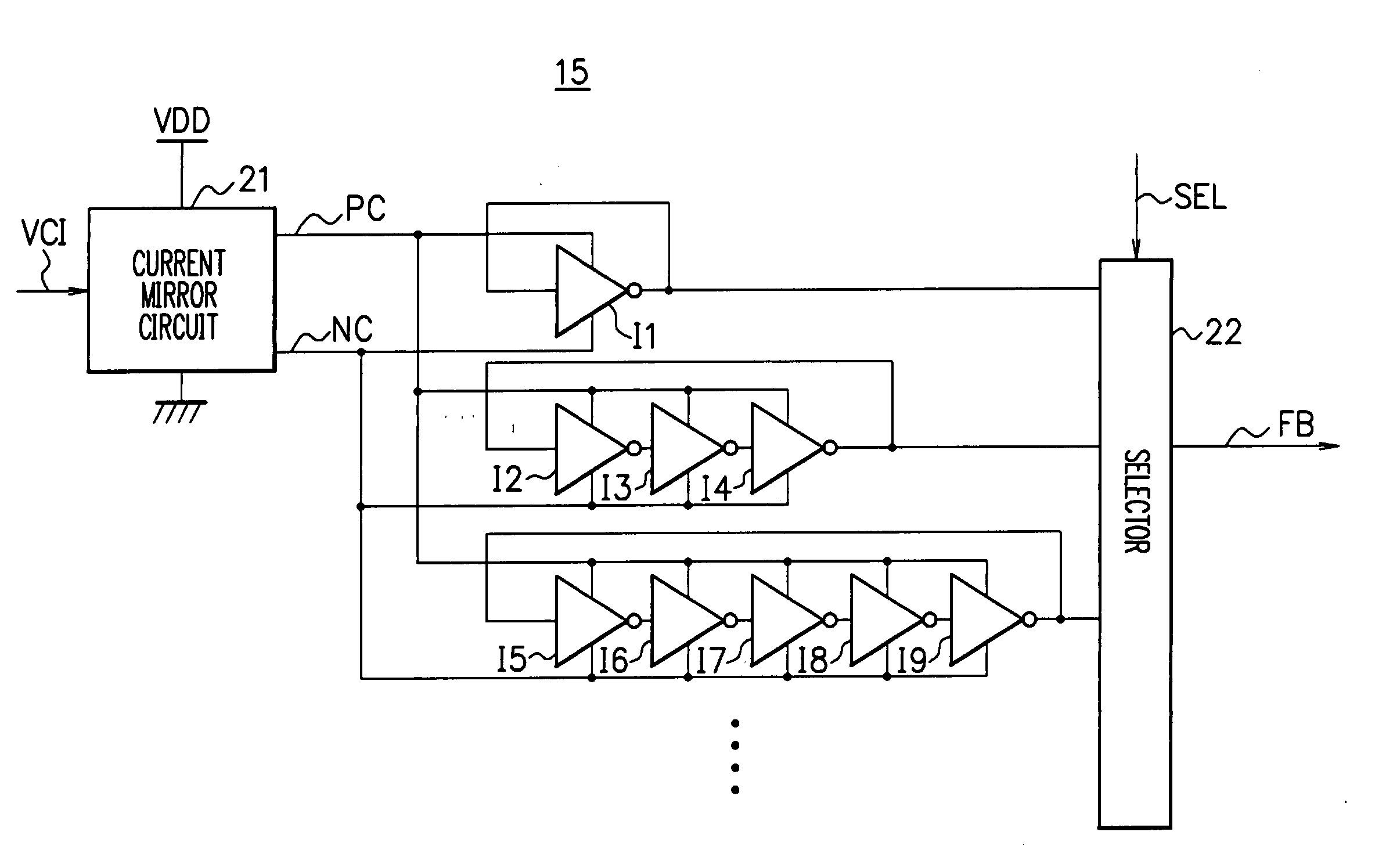
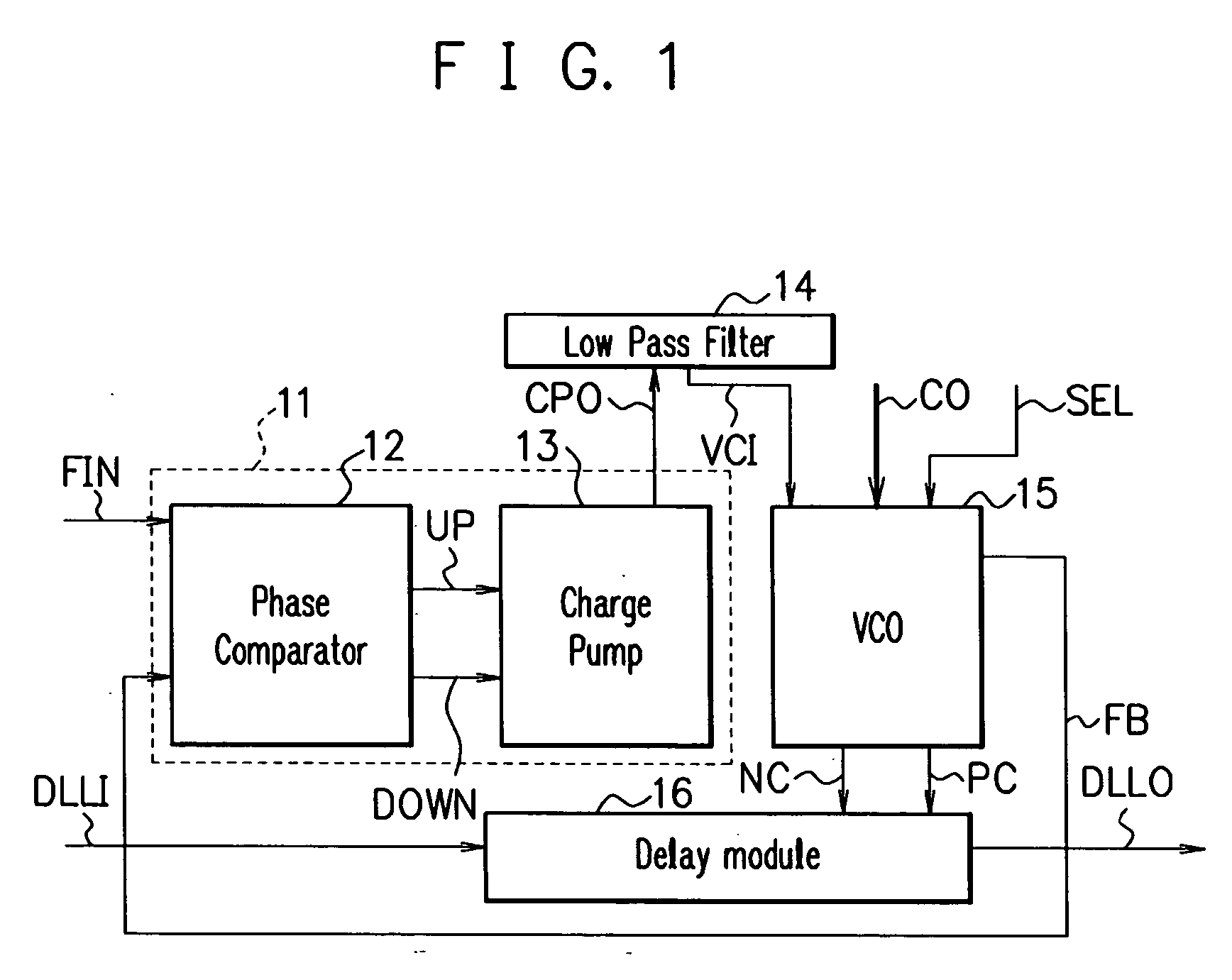
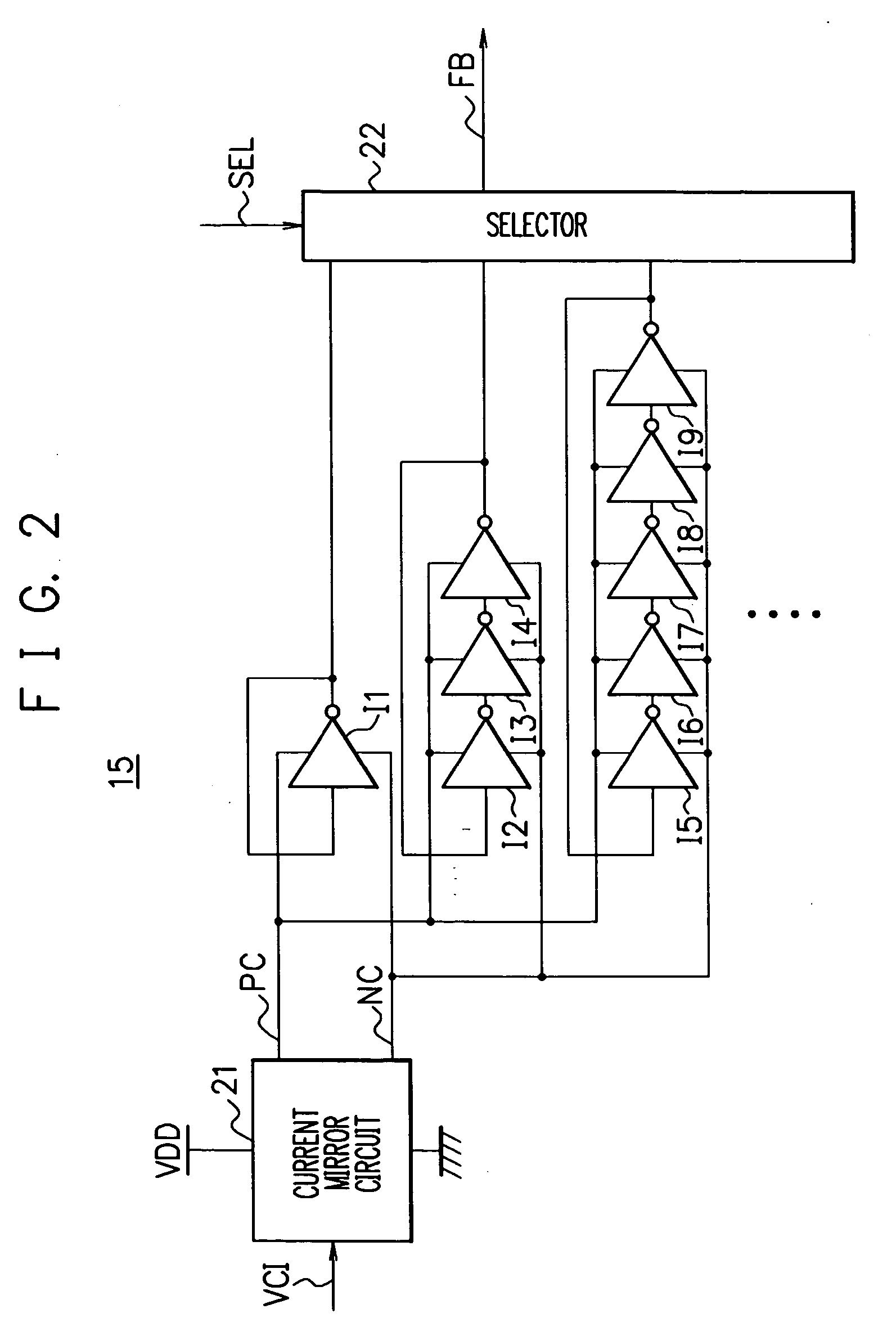
[0032]FIG. 1 is a block diagram showing a configuration example of a DLL (delay locked loop) circuit to which a semiconductor device according to an embodiment of the present invention is applied. The DLL circuit in this embodiment includes a phase comparing circuit 11, a filter circuit (Low Pass Filter) 14, a voltage-controlled oscillation circuit (VCO) 15, and a delay circuit (Delay module) 16.

[0033] To the phase comparing circuit 11, a reference clock signal FIN and a delay clock signal FB which is a feedback clock signal are inputted. Here, the reference clock signal FIN is an externally supplied signal, while the delay clock signal FB is a signal supplied from the voltage-controlled oscillation circuit 15. The phase comparing circuit 11 compares phases of these two clock signals FIN and FB to output a voltage signal CPO to the filter circuit 14 according to the comparison result. ...


PUM


Abstract

A voltage-controlled oscillation circuit (15) includes a plurality of independent ring oscillation circuits different in the number of stages; and a selector (22) selectively outputting as a feedback clock signal (FB) an output of one of the ring oscillation circuits, so that any of the outputs of the independent ring oscillation circuits is always outputted as the feedback clock signal, which makes it possible to output the feedback clock signal keeping a proper duty ratio even when the operating speed is high, allowing arbitrary adjustment of the delay time before an input signal (DLLI) is outputted.

Description

TECHNICAL FIELD [0001] The present invention relates to a semiconductor device and a voltage-controlled oscillation circuit, and more particularly, is suitable for use as a DLL (Delay Locked Loop) circuit. BACKGROUND ART [0002] A DLL (Delay Locked Loop) circuit is used as an interface or the like of a memory, such as a DDR (Double Data Rate) memory, to / from which data is writable / readable in synchronization with a clock signal. The DLL circuit utilizes a PLL (Phase Locked Loop) function to adjust the delay time (output delay) before an inputted signal is outputted. Specifically, the DLL circuit compares an externally supplied reference clock signal and a clock signal generated in an internal voltage-controlled oscillation circuit to control the oscillation frequency of the clock signal, and adjusts the delay time by using a signal relating to this control. [0003] However, a semiconductor device such as the DLL circuit generally has only one voltage-controlled oscillation circuit. Th...

Claims


Application Information

Patent Timeline
Patent Type & Authority Applications(United States)
IPC IPC(8): H03L7/00H03K3/03H03K3/354H03K5/13H03K19/017H03L7/081H03L7/099
CPCH03K3/0315H03K5/133H03L7/0805H03L7/0995
Inventor YAMANAKA, HIROAKIKOUSAKA, KUNIMITSUNISHIWAKI, KIYOSHI
Owner SOCIONEXT INC
Learn More