Off-chip data relocation

Active Publication Date: 2006-06-22
SANDISK TECH LLC
View PDF38 Cites 121 Cited by
  • Summary
  • Abstract
  • Description
  • Claims
  • Application Information

AI Technical Summary

Benefits of technology

[0025] According to one principal aspect of the present invention, briefly and generally, the on-chip copy process is extended so that the data may be copied between two blocks that may be on different chips, different planes on the same chip, or the same plane of the same chip. More specifically, the methods described here provide a singl

Problems solved by technology

Prior art methods describe the data relocation operation as a consecutive data read, then data integrity check and error correction, if necessary, before writing the data to a new location, so that there is a high constant performance penalty of data transfer and verification.
The integrity check is done concurrently with the data write so that, in the case of error, there is a high probability of the need to rewrite the entire block with a high penalty in performance and time-out/latency.
However, the performance co

Method used


Image

  • Off-chip data relocation
  • Off-chip data relocation
  • Off-chip data relocation

Examples


Embodiment Construction

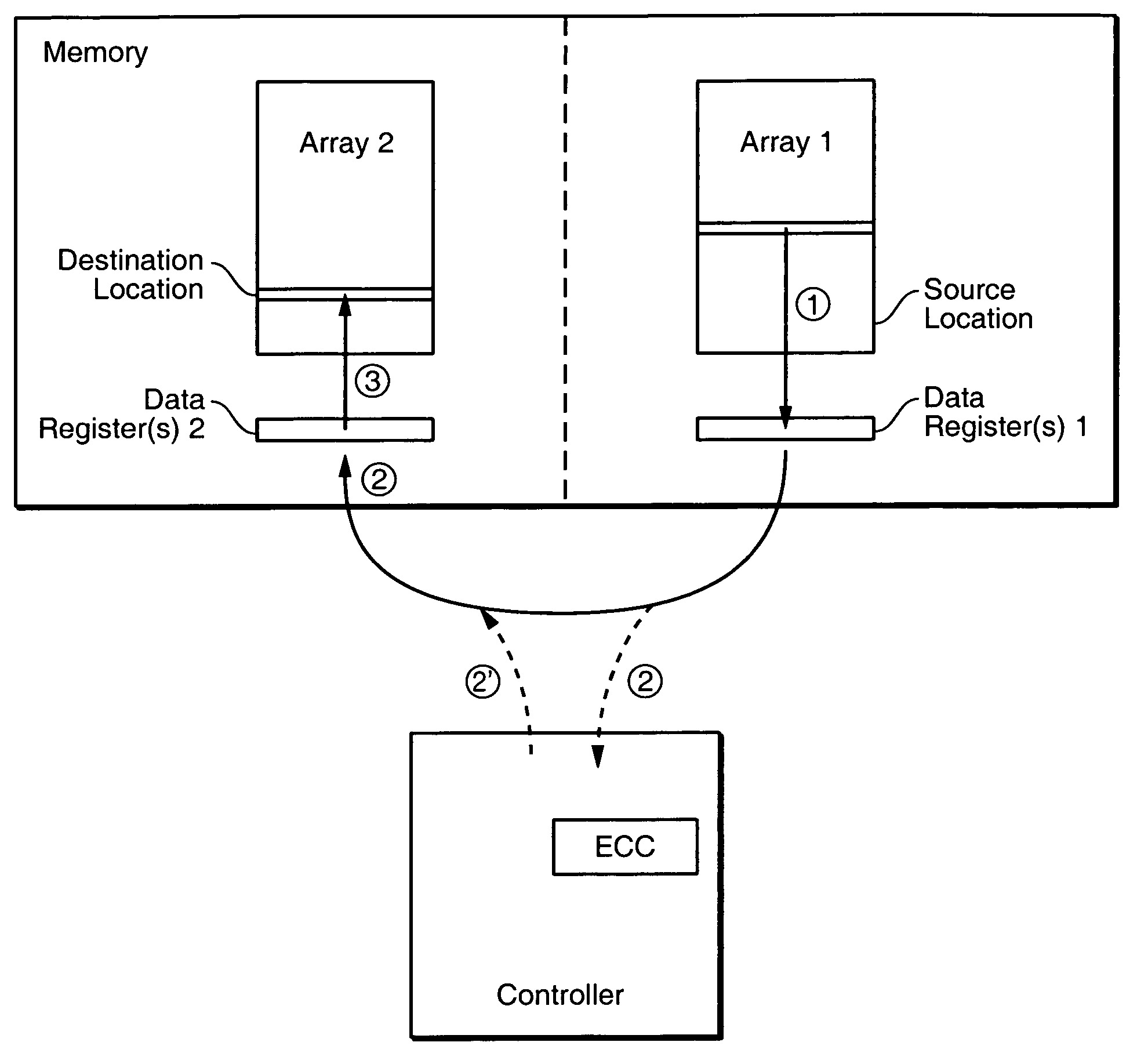
[0044] In a first aspect, the present invention generalizes the copy operation to allow data to be copied between two memory blocks that may be on two different chips, on two planes on the same chip, or as well as on the same plane of the same chip. Consequently, the methods described here provide a single data copying mechanism that allows data to be copied between any two locations in a flash or other memory array. The performance for the more general copy is the same as for on-chip copy as it is generally applied in the prior art. Removing the restrictions on data location, result in improved algorithm operations that reduce the frequency of copying data.

[0045] Generally, the method described here allows data in memory block to be copied to another memory block that may be:

[0046] 1) In a different chip;

[0047] 2) In a different plane of the same chip; or

[0048] 3) In the same plane of the same chip.

[0049] To support this functionality, the control logic and data paths within t...


PUM


Abstract

The on-chip copy process is extended so that the data may be copied between two blocks that may be on different chips, different planes on the same chip, or the same plane of the same chip. More specifically, the methods described here provide a single data copying mechanism that allows data to be copied between any two locations in a memory system. An exemplary embodiment uses an EDO-type timing. According to another aspect, selected portions of the relocated data, such as chosen words in a transferred page, can be updated in the controller on the fly. In addition to transferring a data set directly from a read buffer of a source array to a write buffer of a destination array, the data set can concurrently be copied, if desired, into the controller where an error detection and correction operation can be performed on it.

Description

BACKGROUND OF THE INVENTION [0001] This invention pertains to the field of semiconductor non-volatile data storage system architectures and their methods of operation, and has application to data storage systems based on flash electrically erasable and programmable read-only memories (EEPROMs) and other types of memory system. [0002] A common application of flash EEPROM devices is as a mass data storage subsystem for electronic devices. Such subsystems are commonly implemented as either removable memory cards that can be inserted into multiple host systems or as non-removable embedded storage within the host system. In both implementations, the subsystem includes one or more flash devices and often a subsystem controller. [0003] Flash EEPROM devices are composed of one or more arrays of transistor cells, each cell capable of non-volatile storage of one or more bits of data. Thus flash memory does not require power to retain the data programmed therein. Once programmed however, a cel...

Claims


Application Information

Patent Timeline
IPC IPC(8): G06F12/16
CPCG11C16/10G11C16/26G11C16/06G11C7/10G11C16/32
Inventor CONLEY, KEVIN M.SMITH, PETER JOHN
Owner SANDISK TECH LLC
Why Eureka
Try Eureka