Semiconductor device and manufacturing method thereof

Inactive Publication Date: 2006-06-29
ELPIDA MEMORY INC
View PDF7 Cites 10 Cited by
  • Summary
  • Abstract
  • Description
  • Claims
  • Application Information

AI Technical Summary

Benefits of technology

[0018] As described above, according to the present invention, such an insulating film is provided on a semiconductor substrate that has sufficient adhesion to a chalcogenide-based phase change material, a chalcogenide film is embedded in holes formed in the insulating film, and it is thereby possible to effectively prevent delamination of the chalcogenide film in the manufacturin

Problems solved by technology

However, in the cross-sectional structure as shown in FIG. 15A, it is known that adhesion is generally poor between the chalcogenide film 202 and the silicon oxide film 201.
However, in this method, elements contained in the adhesive layer diffuse into the chalcogenide film 202, and thereby the composition of the chalcogenide film 202 changes and causes deterioration in characteristics.
In other words, when the distance between adjacent bi

Method used


Image

  • Semiconductor device and manufacturing method thereof
  • Semiconductor device and manufacturing method thereof
  • Semiconductor device and manufacturing method thereof

Examples


Example

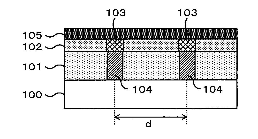
[0035] An embodiment of the present invention will specifically be described below with reference to accompanying drawings. This embodiment describes non-volatile phase change memory using chalcogenide-based phase change material as an example of a semiconductor device to which the invention is applied.

[0036] A basic structure of the phase change memory of this embodiment will be described below. FIG. 1 is a view showing a schematic cross-sectional structure of the phase change memory of this embodiment, and corresponds to FIG. 15A showing a conventional structure. In FIG. 1, MOS transistors (not shown) are formed on a semiconductor substrate 100, and a silicon oxide film 101 is formed on the substrate as an insulating film. A silicon nitride film 102 is formed on the silicon oxide film 101. In the silicon nitride film 102, holes are respectively formed at a plurality of bit areas spaced a distance d from each other, and a chalcogenide film 103 is embedded in each bit area. The cha...


PUM


Abstract

A semiconductor device having a plurality of phase change devices rewritably storing data, comprising: an insulating film deposited on a semiconductor substrate using an insulating material having sufficient adhesion to a chalcogenide-based phase change material; a chalcogenide film formed by embedding the chalcogenide-based phase change material in a hole formed at each of bit areas separated from each other in the insulating film; and an electrode structure for supplying a current to each the phase change device made of the chalcogenide film in the bit area.

Description

BACKGROUND OF THE INVENTION [0001] 1. Field of the Invention [0002] The present invention relates to a semiconductor device using chalcogenide-based phase change material as a memory device and a method of manufacturing the semiconductor device. [0003] 2. Related Art [0004] In regards to non-volatile memory widely used as data storage means of portable devices or the like, attention is paid to phase change memory using structural changes of phase change material as a next-generation technology. The phase change memory has a structure in which a memory device is formed on a semiconductor substrate using a chalcogenide-based phase change material such as germanium, antimony and tellurium, and is heated. Such a structure causes the phase change material to transition freely between its high-resistance amorphous state and low-resistance crystalline state and enables to rewritably store data (for example, see U.S. Pat. No. 6,590,807 B2 and U.S. Pat. No. 6,567,296B1). [0005]FIG. 15A shows...

Claims


Application Information

Patent Timeline
IPC IPC(8): H01L29/768
CPCH01L45/06H01L45/1233H01L45/126H01L45/144H01L27/2436H01L45/1683H10B63/30H10N70/231H10N70/826H10N70/8413H10N70/8828H10N70/066
Inventor KAWAGOE, TSUYOSHIASANO, ISAMU
Owner ELPIDA MEMORY INC
Why Eureka
Try Eureka