Method for fabricating vertical CMOS image sensor

a technology of image sensor and cmos, which is applied in the direction of electrical equipment, semiconductor devices, radio frequency controlled devices, etc., can solve the problems of relative severe lateral diffusion, deterioration of isolation characteristics between adjacent photodiodes, so as to improve integration and reduce the size of the unit pixel

Active Publication Date: 2006-06-29
DONGBU HITEK CO LTD
View PDF28 Cites 23 Cited by
  • Summary
  • Abstract
  • Description
  • Claims
  • Application Information

AI Technical Summary

Benefits of technology

[0016] An object of the present invention is to provide a method for fabricating a vertical CMOS image sensor (which generally improves integration and decreases the size of the unit pixel by minimizing the lateral diffusion of a plug implant), in which phosphorous and arsenic ions are implanted at a controlled dose and energy.

Problems solved by technology

At sufficiently high doses, there may be relatively severe lateral diffusion.
Thus, the isolation characteristics between adjacent photodiodes may deteriorate.
In the aforementioned vertical CMOS image sensor according to the related art, the isolation characteristics between adjacent photodiodes may deteriorate due to the lateral diffusion of the first plug.
Accordingly, it can be difficult to decrease the size of unit pixel due to the deterioration of the isolation characteristics.
Thus, it may have a limitation with regard to decreasing the size of the unit pixel due to the potential deterioration of the isolation characteristics.
As a result, it can be difficult to obtain (or realize the potential for) high integration of the vertical CMOS image sensor, and thus decrease the production cost.

Method used


Image

  • Method for fabricating vertical CMOS image sensor
  • Method for fabricating vertical CMOS image sensor
  • Method for fabricating vertical CMOS image sensor

Examples


Embodiment Construction

[0026] Reference will now be made in detail to the preferred embodiments of the present invention, examples of which are illustrated in the accompanying drawings. Wherever possible, the same reference numbers will be used throughout the drawings to refer to the same or like parts.

[0027] Hereinafter, a method for fabricating a vertical CMOS image sensor according to the present invention will be described with reference to the accompanying drawings.

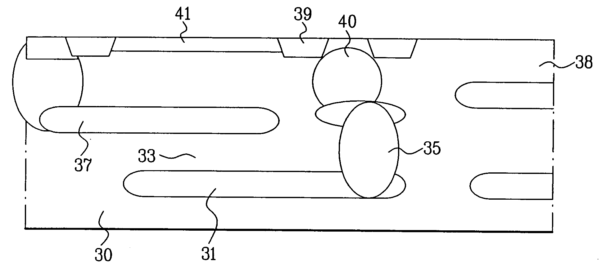
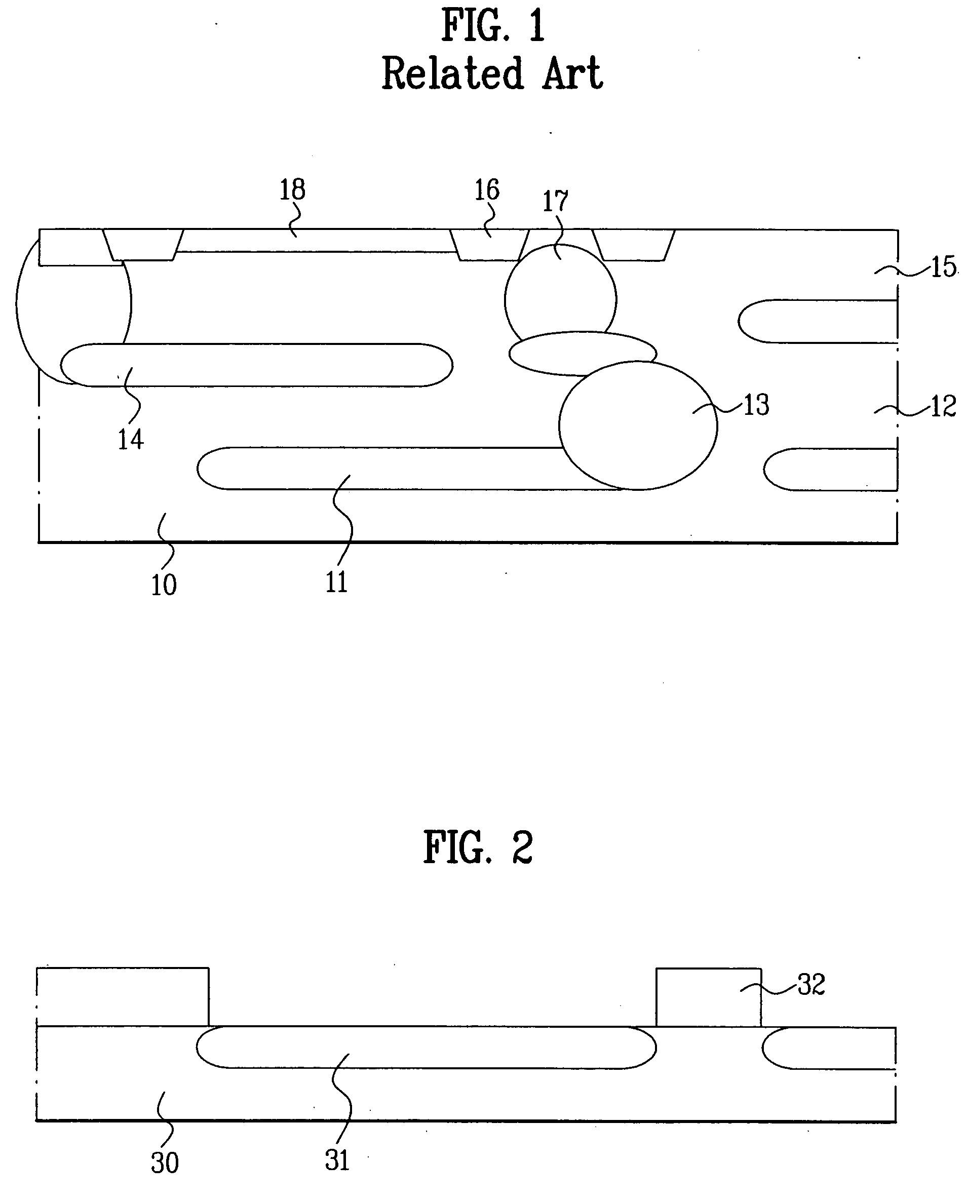
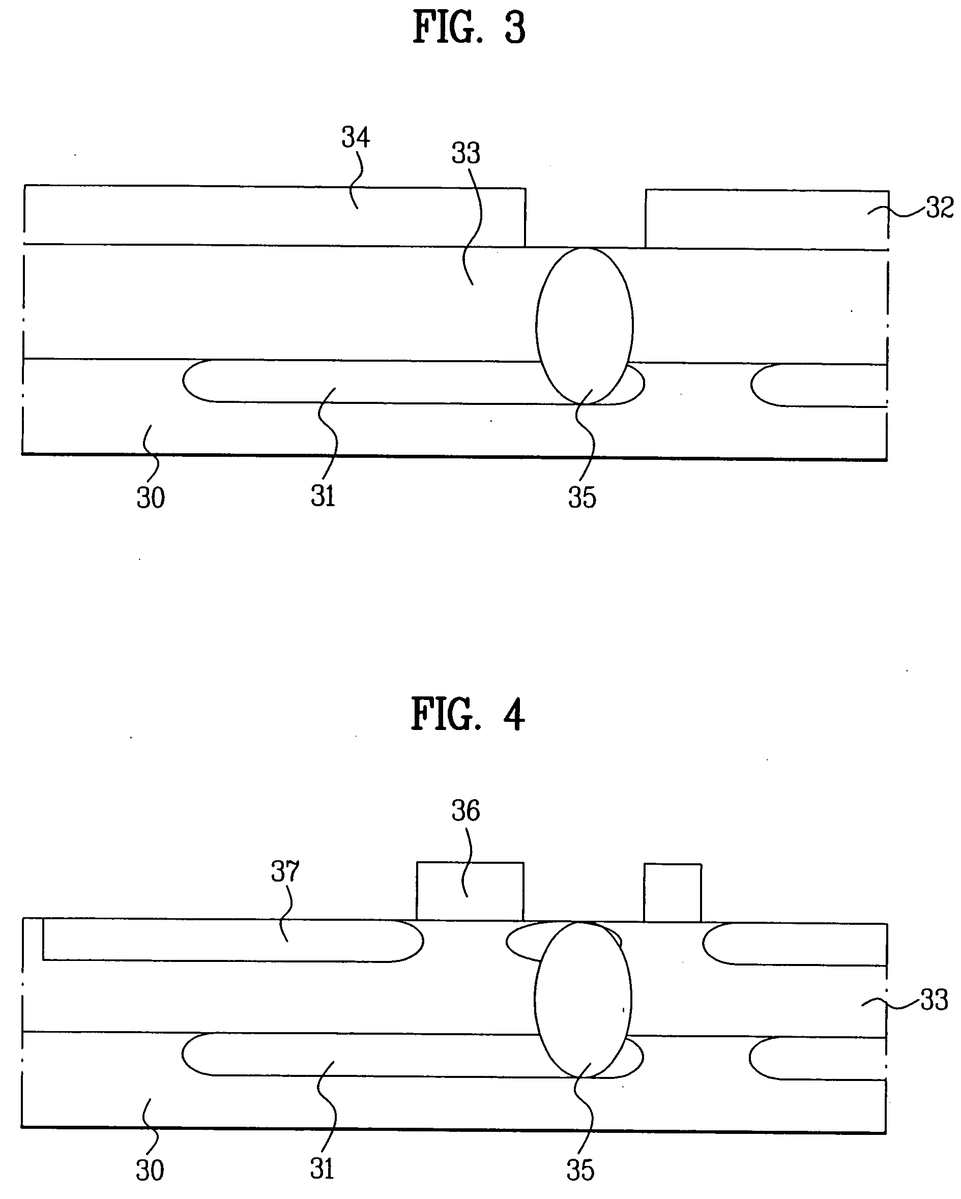
[0028] FIGS. 2 to 5 illustrate cross sectional views of a method for fabricating a vertical CMOS image sensor according to the present invention.

[0029] Referring to FIG. 2, a first epitaxial layer may be grown (typically by conventional epitaxial growth of silicon or silicon-germanium) on a semiconductor substrate 30, and a first photoresist is coated on the semiconductor substrate 30 including the first epitaxial layer. (Alternatively, a single crystal silicon substrate having certain predetermined qualities or characteristics, perhaps...


PUM


Abstract

A method of fabricating a vertical CMOS image sensor is disclosed, to improve the integration with the decrease in size of pixel by minimizing the lateral diffusion, in which phosphorous and arsenic ions are implanted while controlling the dose and energy, the method including forming a first photodiode in a semiconductor substrate; forming a first epitaxial layer on the semiconductor substrate; forming a first plug by sequentially implanting first and second ions in the first epitaxial layer; forming a second photodiode in the first epitaxial layer; forming a second epitaxial layer in the first epitaxial layer; forming an isolation area in the second epitaxial layer; and forming a third photodiode and a second plug in the second epitaxial layer.

Description

[0001] This application claims the benefit of Korean Patent Application No. P2004-114603, filed on Dec. 29, 2004, which is hereby incorporated by reference as if fully set forth herein. BACKGROUND OF THE INVENTION [0002] 1. Field of the Invention [0003] The present invention relates to a method for fabricating a vertical CMOS image sensor, and more particularly, to a method for fabricating a vertical CMOS image sensor that reduces or minimizes the lateral diffusion in an (implant) plug by controlling the kind (or element), dose and energy of ion implantation. [0004] 2. Discussion of the Related Art [0005] Generally, an image sensor is a semiconductor device for converting an optical image to an electric signal. Image sensors may be classified into charge-coupled devices (CCDs) and CMOS image sensors. In the case of the CCD, metal-oxide-silicon MOS capacitors are positioned adjacent to one another, and electric carriers are stored in and transferred from the MOS capacitors. In the CM...

Claims


Application Information

Patent Timeline
Patent Type & Authority Applications(United States)
IPC IPC(8): H01L21/336H01L29/76
CPCH01L27/14603H01L27/1463H01L27/14647H01L27/14689H01L27/146H01L31/10
Inventor LEE, SANG GI
Owner DONGBU HITEK CO LTD
Why Eureka
Try Eureka