Method for fabricating a CMOS image sensor

a technology of image sensor and metal oxide semiconductor, which is applied in the direction of semiconductor devices, diodes, radiation controlled devices, etc., can solve the problems of difficult control circuit, high power consumption, and difficult signal processing circuit, and achieve the effect of improving the performance and yield of the image sensor

Inactive Publication Date: 2006-06-29
DONGBU ELECTRONICS CO LTD
View PDF8 Cites 11 Cited by
  • Summary
  • Abstract
  • Description
  • Claims
  • Application Information

AI Technical Summary

Benefits of technology

[0036] An advantage of the present invention is that it provides a method for fabricating a CMOS image sensor, in which electron shower is performed for microlenses whose surfaces are charged to have a positive potential, so as to neutralize the conducted potential, thereby improving performance and yield of the image sensor.
[0037] Additional advantages and features of the invention will be set forth in part in the description which follows and in part will become apparent to those having ordinary skill in the art upon examination of the following or may be learned from practice of the invention. These and other advantages of the invention may be realized and attained by the structure particularly pointed out in the written description and claims hereof as well as the appended drawings.
[0038] To achieve these and other advantages and in accordance with the purpose of the invention, as embodied and broadly described herein, a method for fabricating a CMOS image sensor includes forming a metal pad in a pad area over a semiconductor substrate divided into an active area and the pad area, forming a passivation layer on an entire surface of the semiconductor substrate including the metal pad, selectively removing the passivation layer to expose the metal pad, thereby forming a metal pad open portion, forming a barrier layer on the entire surface of the semiconductor substrate including the metal pad open portion, forming R, G and B color filter layers over the barrier layer of the active area, forming microlenses over the color filter layers, removing the barrier layer of the pad area, and performing electron shower to neutralize positive potential trapped in the microlenses.
[0039] The barrier layer is removed by reactive ion etching (RIE). When the barrier layer is removed by the RIE, curing is performed using N2 gas to remove a corrosive material that may remain on a surface of the metal pad.
[0040] The method may further include forming an insulating layer on the semiconductor substrate prior to forming the metal pad the semiconductor substrate.
[0041] The method may further include forming first planarization layers on the barrier layer of the active area before forming color filter layers over the barrier layer of the active area and forming second planarization layers on the color filter layers before forming the microlenses over the color filter layers.

Problems solved by technology

The CCD has drawbacks in its fabrication process because of a complicated driving mode, high power consumption, and multistage photolithographic processes.
Also, it is difficult for a control circuit, a signal processing circuit, and an analog-to-digital converter to be integrated in a CCD chip and still obtain a slim size product.
The related art CMOS image sensor has several problems.
For this reason, a problem occurs in that the metal pad is corroded to cause a pit, thereby deteriorating reliability of the image sensor along with its yield.
As a result, performance of the image sensor is deteriorated and its yield is reduced.

Method used


Image

  • Method for fabricating a CMOS image sensor
  • Method for fabricating a CMOS image sensor
  • Method for fabricating a CMOS image sensor

Examples


Embodiment Construction

[0055] Reference will now be made in detail to exemplary embodiments of the present invention, examples of which are illustrated in the accompanying drawings. Wherever possible, the same reference numbers will be used throughout the drawings to refer to the same or like parts.

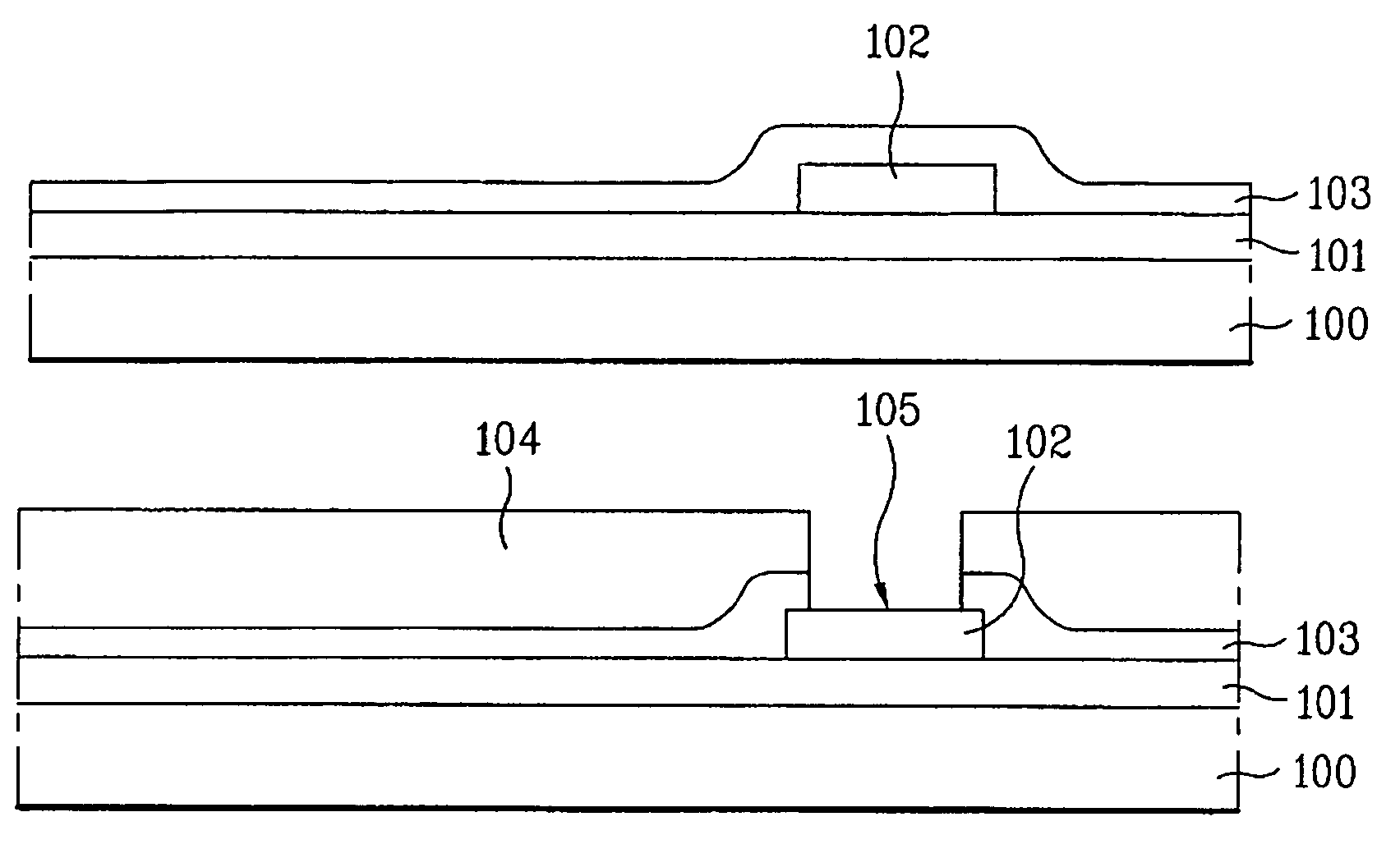
[0056]FIG. 4A to FIG. 4G are sectional views illustrating a method for fabricating a CMOS image sensor according to the an exemplary embodiment of the present invention.

[0057] As shown in FIG. 4A, an insulating layer 101 such as a gate insulating layer or an interlayer insulating layer is formed on a semiconductor substrate 100. A metal pad 102 of each signal line is formed on the insulating layer 101. The metal pad 102 may be formed of the same material as that of respective gate electrodes 120, 130 and 140 shown in FIG. 2 on the same layer as the gate electrodes 120, 130 and 140. Alternatively, the metal pad 102 may be formed of a material different from that of the gate electrodes 120, 130 and 140 through ...


PUM


Abstract

A method for fabricating a CMOS image sensor in which an electron shower is performed for microlenses whose surfaces are charged to a positive potential, so as to neutralize the positive potential, thereby improving performance and yield of the image sensor.

Description

CROSS-REFERENCE TO RELATED APPLICATIONS [0001] This application claims the benefit of the Korean Patent Application No. P2004-112027, filed on Dec. 24, 2004, which is hereby incorporated by reference as if fully set forth herein. BACKGROUND OF THE INVENTION [0002] 1. Field of the Invention [0003] The present invention relates to a complementary metal-oxide semiconductor (CMOS) image sensor, and more particularly, to a CMOS image sensor and a method for fabricating the same, in which the performance of the CMOS image sensor is improved and, at the same time, its yield is improved. [0004] 2. Discussion of the Related Art [0005] An image sensor is a semiconductor device that converts optical images to electrical signals. The image sensor is classified into a charge coupled device (CCD) and a CMOS image sensor. [0006] The CCD has drawbacks in its fabrication process because of a complicated driving mode, high power consumption, and multistage photolithographic processes. Also, it is dif...

Claims


Application Information

Patent Timeline
Patent Type & Authority Applications(United States)
IPC IPC(8): H01L21/00
CPCH01L27/14609H01L27/14621H01L27/14627H01L27/14643H01L27/14685H01L27/146H01L31/10
Inventor LIM, BI O.
Owner DONGBU ELECTRONICS CO LTD
Why Eureka
Try Eureka