Method And Related Apparatus For Realizing Two-Port Synchronous Memory Device

a synchronous memory and multi-port technology, applied in the field of multi-port synchronous memory devices, can solve the problems of requiring more complex circuit structures, occupying a larger layout area of two-port memory, and achieving the effect of two-port static random access memory with a large layout area, and achieving small layout area, low cost, and small layout area

Inactive Publication Date: 2006-06-29
VIA TECH INC
View PDF6 Cites 6 Cited by
  • Summary
  • Abstract
  • Description
  • Claims
  • Application Information

AI Technical Summary

Benefits of technology

[0015] In a single-port memory, each memory cell of the single-port memory comprise only one accessing port. Therefore, the single-port memory can have a small layout area and low cost. Typically, each memory cell of the single-port SRAM comprises 6 transistors (6T) or comprises 4 transistors and 2 resistors (2R4T). The two-port SRAM comprises 8 transistors (8T) or comprises 6 transistors and 2 resistors (2R6T). Comparing the two memories, it can be seen that the single-port memory has a smaller layout area and lower cost. Therefore, the present invention can achieve the functions of the more costly and larger two-port synchronous memory device by utilizing less expensive and smaller single-port memory.

Problems solved by technology

However, in the prior art, the two-port synchronous memory device is achieved by a two-port static random access memory with a high cost and a large layout area.
This causes the two-port memory to occupy a larger layout area, require more complex circuit structure, and cost more to produce and design.
Therefore, the two-port synchronous memory device achieved by the above-mentioned two-port memory is not widely utilized due to its disadvantages.

Method used


Image

  • Method And Related Apparatus For Realizing Two-Port Synchronous Memory Device
  • Method And Related Apparatus For Realizing Two-Port Synchronous Memory Device
  • Method And Related Apparatus For Realizing Two-Port Synchronous Memory Device

Examples


second embodiment

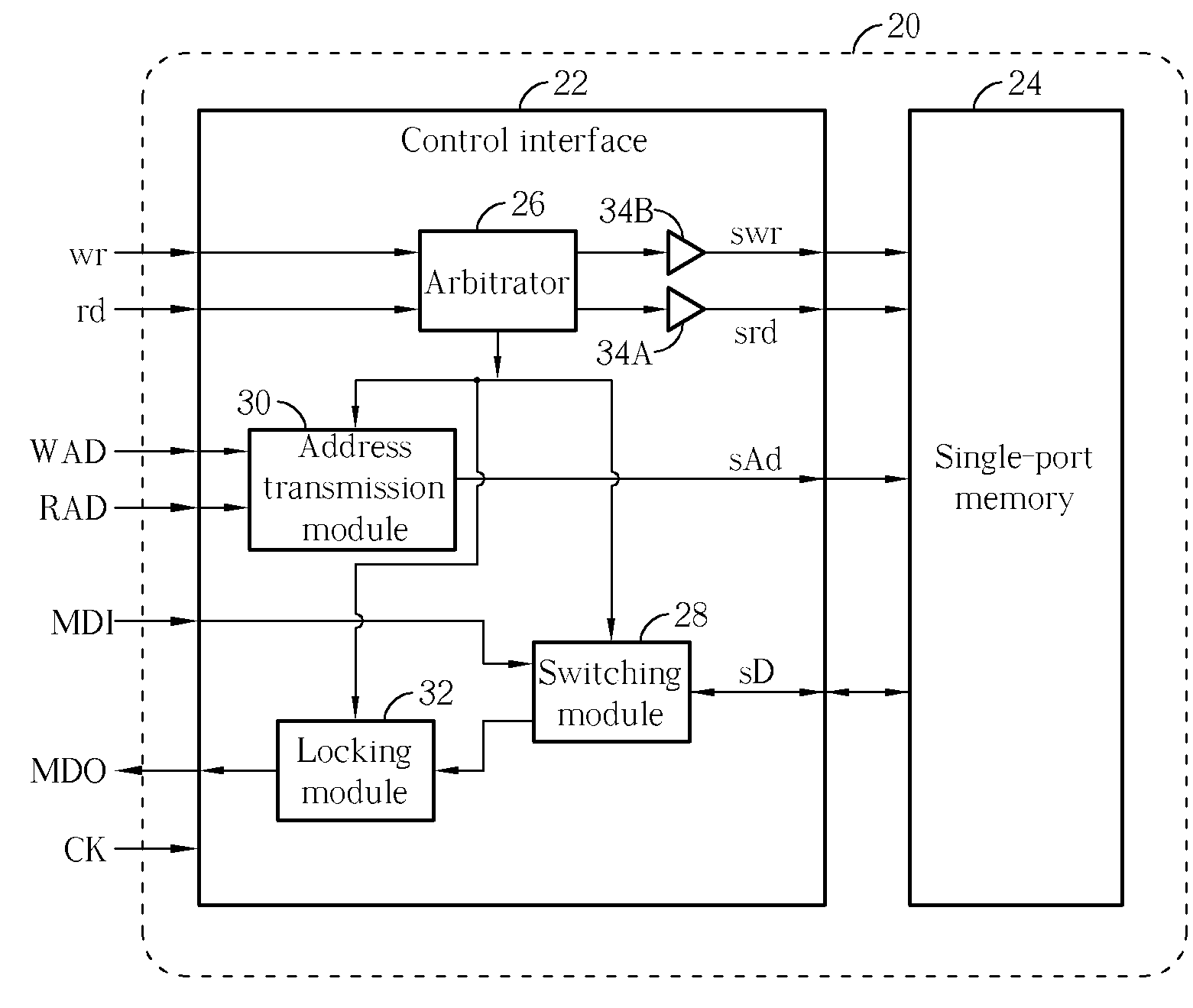
[0033] In the present invention, a clock having double frequency triggers the single-port memory. Please refer to FIG. 5, showing a block diagram of a memory device 40 of another embodiment according to the present invention. The memory device 40 also comprises a control interface 42 and a single-port memory 46 to achieve the function of the two-port synchronous memory device. In this embodiment, the control interface 42 comprises a clock generator 48, delay units 60A and 60B, two scheduling units 54A and 54B, an address transmission module 50, a switching module 58, and a locking module 52. Please note that the clock generator 48 can be a phase lock loop for generating a clock CK2 whose frequency is double that of the clock CK (the clock period of the clock CK is half of the clock period of the clock CK). The clock CK2 is utilized to trigger the operational timings of the single-port memory 46. Under the triggers of the clock CK2, the single-port memory 46 can receive a reading com...

first embodiment

[0034] In the control interface 42, the scheduling units 54A and 54B can determine whether the external signals wr and rd are transferred to the delay units 60A and 60B through the signals swr0 and swr0 to generate corresponding signals swr and srd. In the actual implementation, the scheduling units 54A and 54B can be achieved by AND gates. When the external signals wr and rd are enabled to a high level in the same period of the clock CK, the scheduling unit 54A can perform an AND operation on the clock CK and the signal rd. This causes the high level of the signal rd to be transferred to the delay unit 60A in the first half clock period (the high level of the clock). Additionally, the scheduling unit 54B can perform an AND operation on an inversed clock, which is inversed by an inverter inv shown in FIG. 5 This causes the high level of the signal wr to be transferred to the delay unit 60B in the last half clock period. In other words, the scheduling units 54A and 54B can be respect...


PUM


Abstract

Method and related apparatus for realizing a two-port synchronous memory device with a single-port memory. Clock-triggered two-port synchronous memory device can synchronously receive reading and writing commands within a clock period to simultaneous execute these two commands, while a single port memory must execute a single reading and writing command sequentially. Since a single-port memory features a lower cost and a smaller layout area, the invention realizes a two-port synchronous memory device by making a single-port memory first execute one of the reading/writing commands and then the other command within a single clock period, such that the two commands are completed after a single clock period. Thus a two-port synchronous memory device can be realized with a single-port memory.

Description

BACKGROUND OF INVENTION [0001] 1. Field of the Invention [0002] The invention relates to a method and related apparatus for realizing a multi-port synchronous memory device, and more particularly, to a method and related apparatus for utilizing a single-port memory of low cost and small layout area to realize a multi-port synchronous memory device. [0003] 2. Description of the Prior Art [0004] In today's society, data, information, documents, and videos can be processed, transferred, managed, and stored in an electronic form (especially a digital electronic form). Therefore, electronic circuits for transferring electronic signals and managing electronic data become key points of design. This is especially true of widely utilized multi-port synchronous memory devices that can read / write data synchronously. The multi-port synchronous memory devices can be triggered by a clock such that the memory devices can synchronously receive and complete the execution of a reading command and a w...

Claims


Application Information

Patent Timeline
Patent Type & Authority Applications(United States)
IPC IPC(8): G06F13/28
CPCG06F13/1605
Inventor CHEN, SHENG-CHUNGHSU, JUNG-TSAN
Owner VIA TECH INC
Why Eureka
Try Eureka