Controlling melt-solid interface shape of a growing silicon crystal using a variable magnetic field

a technology of melting solid and growing crystals, applied in the direction of crystal growth process, polycrystalline material growth, under a protective fluid, etc., can solve the problems of increasing the mechanical strength of silicon wafers, destroying radial uniformity, and devices with inferior performance characteristics, so as to achieve more flexibility and capability, the effect of avoiding deficiencies

Active Publication Date: 2006-07-06
GLOBALWAFERS CO LTD
View PDF14 Cites 23 Cited by
  • Summary
  • Abstract
  • Description
  • Claims
  • Application Information

AI Technical Summary

Benefits of technology

[0011] Embodiments of the invention overcome one or more deficiencies in the prior art and provide control of an interface shape between a melt and a crystal by applying a variable magnetic field. In one embodiment, the invention controls flow within a silicon melt from which a crystal is growing via an asymmetric magnetic field having a configuration and field intensity that may be continuously changed. Embodiments of the invention thus allow manipulation of the crystal-to-melt interface shape, the axial temperature gradient at the interface, and the radial variation of the axial temperature gradient in the crystal at and near the interface to achieve a desired interface shape and value. According to aspects of the invention, a variable asymmetric magnetic field achieves more flexibility and capability than any of the conventional magnetic field configurations in controlling the crystal-to-melt interface shape. Moreover, an embodiment of the invention allows a cusp position of the magnetic field to be moved either above or below the crystal-to-melt interface based on a length of the crystal to maintain a desired melt flow control and uniformity. Without changing hardware setups and physical locations, the variable asymmetric magnetic field of the invention combines the benefits of the conventional magnetic field configurations while avoiding their deficiencies.

Problems solved by technology

In the various heat treatment processes during the manufacture of various electrical devices, the oxygen in the crystal may cause crystal defects such as precipitates, dislocation loops, and stacking faults or it may cause electrically active defects resulting in devices with inferior performance characteristics.
The solid solution of oxygen in the crystal, however, increases the mechanical strength of silicon wafers and the crystal defects may improve the yield of conforming products by entrapping contaminants of heavy metals.
But the axial magnetic field configuration destroys radial uniformity due to its dominant axial field component.
But its non-uniformity both axially and radially and the complex and bulky setup make it difficult to apply the horizontal magnetic field configuration in large diameter Czochralski growth processes.
However, the effectiveness of the cusped magnetic field is decreased at the center of the melt.

Method used


Image

  • Controlling melt-solid interface shape of a growing silicon crystal using a variable magnetic field
  • Controlling melt-solid interface shape of a growing silicon crystal using a variable magnetic field
  • Controlling melt-solid interface shape of a growing silicon crystal using a variable magnetic field

Examples


Embodiment Construction

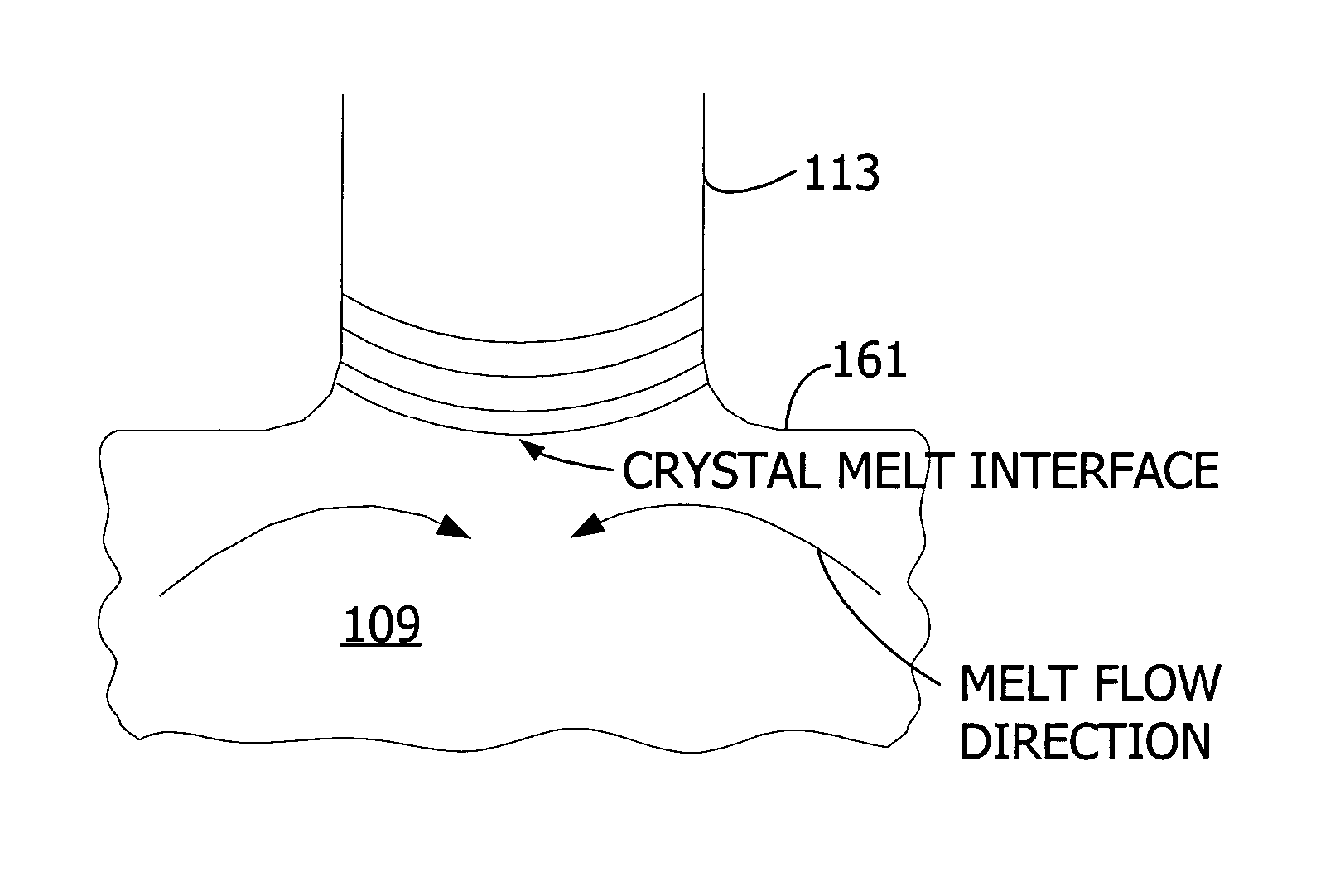
[0040] Referring now to FIG. 4, a Czochralski crystal growth apparatus embodying aspects of the present invention is shown in block diagram form. In general, the crystal growing apparatus includes a vacuum chamber 101 enclosing a crucible 103. Heating means such as a resistance heater 105 surrounds the crucible 103. During heating and crystal pulling, a crucible drive unit (e.g., a motor) 107 rotates crucible 103, for example, in the clockwise direction as indicated by the arrow. The crucible drive unit 107 may also raise and / or lower crucible 103 as desired during the growth process. Within crucible 103 is a silicon melt 109 having a melt level 111. In operation, the apparatus pulls a single crystal 113, starting with a seed crystal 115 attached to a pull shaft or cable 117, from the melt 109. As is known in the art, one end of the pull shaft or cable 117 is connected by way of a pulley (not shown) to a drum (not shown), and the other end is connected to a chuck (not shown) that ho...


PUM

PropertyMeasurementUnit
diameteraaaaaaaaaa
magnetic fieldaaaaaaaaaa

Abstract

Methods and system for controlling crystal growth in a Czochralski crystal growing apparatus. A magnetic field is applied within the crystal growing apparatus and varied to control a shape of the melt-solid interface where the ingot is being pulled from the melt. The shape of the melt-solid interface is formed to a desired shape in response to the varied magnetic field as a function of a length of the ingot.

Description

TECHNICAL FIELD [0001] Embodiments of the present invention relate to the field of producing single crystal silicon used in the manufacture of electronic components. In particular, embodiments of the invention relate to controlling the melt-solid interface shape of a growing crystal by applying a variable magnetic field. BACKGROUND OF THE INVENTION [0002] Single crystal silicon, which is the starting material in most processes for fabricating semiconductor electronic components, is commonly prepared according to the so-called Czochralski process. In this process, polycrystalline silicon, or polysilicon, is charged to a crucible and melted, a seed crystal is brought into contact with the molten silicon, and a single crystal ingot is grown by relatively slow extraction. After formation of a neck is complete, decreasing the pulling rate and / or the melt temperature enlarges the diameter of the crystal until a desired or target diameter is reached. The generally cylindrical main body of ...

Claims


Application Information

Patent Timeline
Patent Type & Authority Applications(United States)
IPC IPC(8): C30B15/00C30B21/06C30B27/02C30B28/10C30B30/04
CPCC30B15/203C30B15/22C30B15/305Y10T117/10Y10S117/917Y10T117/1032Y10T117/1052C30B29/06C30B15/00C30B15/30
Inventor LU, ZHENG
Owner GLOBALWAFERS CO LTD
Why Eureka
Try Eureka