Organic light emitting display (OLED) and its fabrication method

a technology of light-emitting display and organic material, which is applied in the direction of identification means, instruments, lighting and heating apparatus, etc., can solve the problems of reducing the life span and performance of the display

Active Publication Date: 2006-07-06
SAMSUNG DISPLAY CO LTD
View PDF3 Cites 2 Cited by
  • Summary
  • Abstract
  • Description
  • Claims
  • Application Information

AI Technical Summary

Benefits of technology

[0012] The present invention, therefore, provides an Organic Light Emitting Display (OLED) and its fabrication method, in which a pixel defining layer provided on a first electrode includes a gas vent groove, so that gases remaining and condensed in the pixel are vented when an emission layer is formed by a LITI method, thereby completely transferring a donor film to a final transfer region, and preventing an untransferred failure.

Problems solved by technology

Such a failure is called ‘an edge open failure’ or ‘an untransferred failure’, which reduces the life span and performance of the display.

Method used


Image

  • Organic light emitting display (OLED) and its fabrication method
  • Organic light emitting display (OLED) and its fabrication method
  • Organic light emitting display (OLED) and its fabrication method

Examples


Embodiment Construction

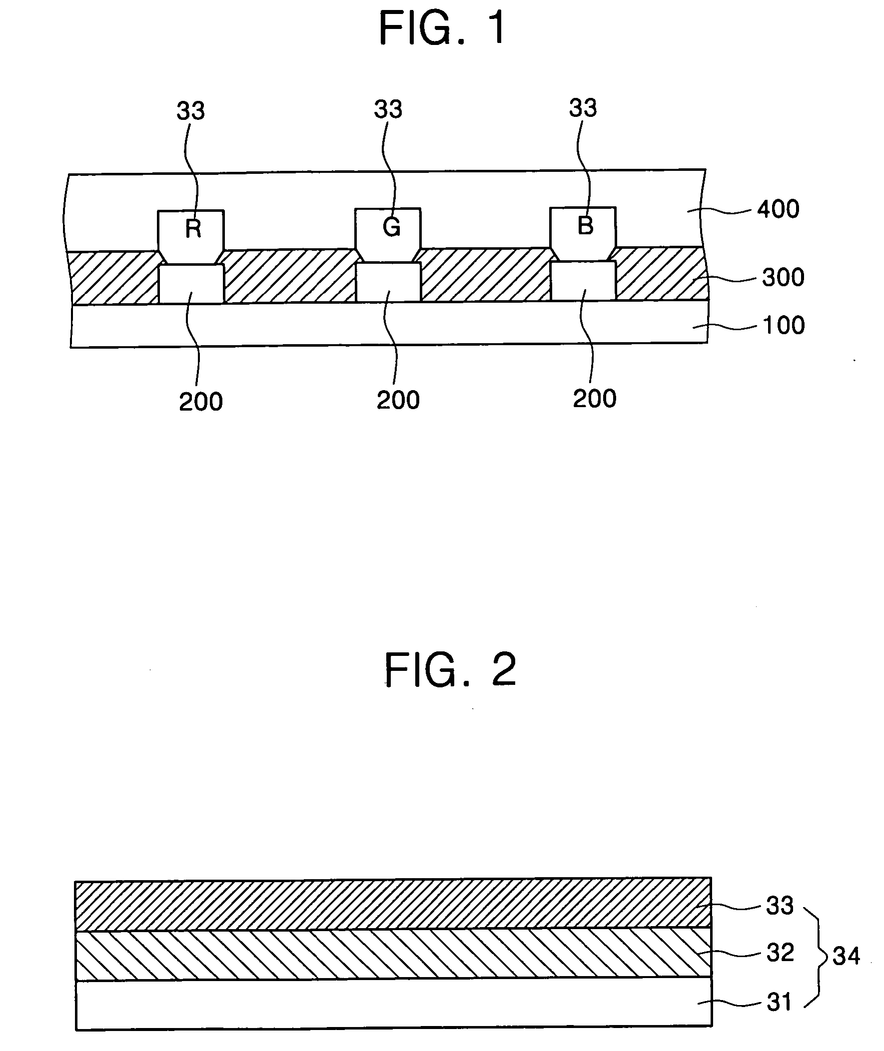
[0033]FIG. 1 is a cross-sectional view of a full-color organic light emitting diode.

[0034] Referring to FIG. 1, a first electrode 200 is patterned on a substrate 100. For a bottom emission organic light emitting diode, the first electrode 200 is a transparent electrode. For a top emission organic light emitting diode, the first electrode is of a transparent conductive material and includes a reflective layer.

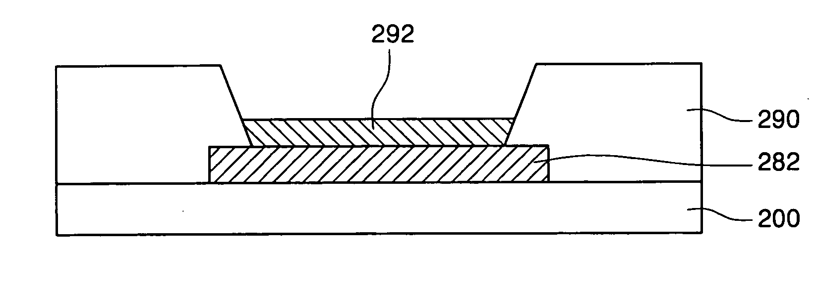
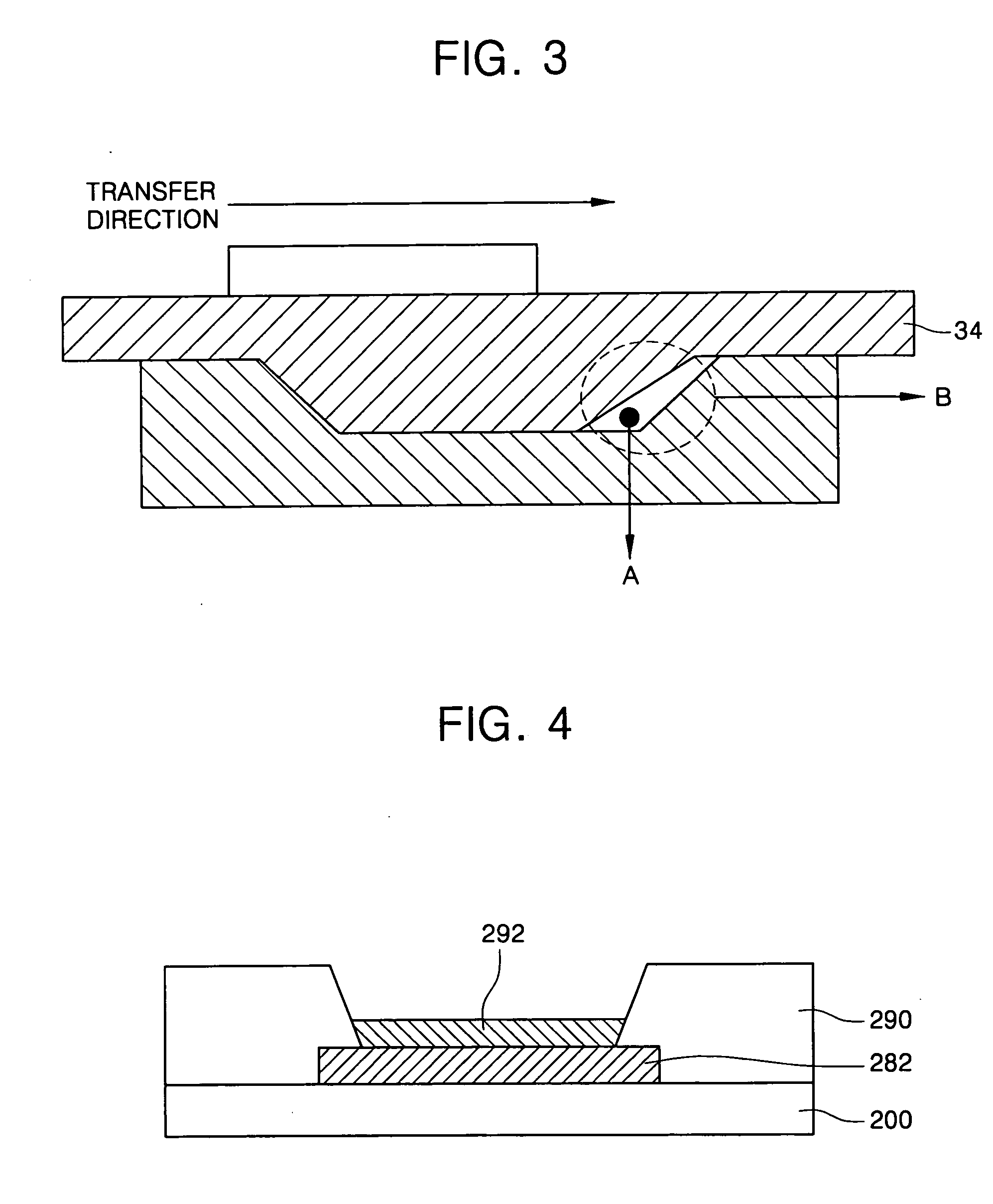
[0035] A Pixel Defining Layer (PDL) 300 is formed of an insulating material on the first electrode 200, thereby defining a pixel region and insulating emission layers from each other.

[0036] In the pixel region defined by the PDL 300, an organic layer including organic emission layers (R, G and B) 33 is formed. Furthermore, the organic layer 33 can further include a hole injection layer, a hole transporting layer, a hole blocking layer, an electron transporting layer, an electron injection layer, etc. The organic emission layer can be formed either of a polymer or a small mole...


PUM

PropertyMeasurementUnit
depthaaaaaaaaaa
temperatureaaaaaaaaaa
thicknessaaaaaaaaaa

Abstract

An Organic Light Emitting Display (OLED) and its fabrication method has a pixel defining layer provided on a first electrode which is formed with a gas vent groove to allow gas to vent when the pixel defining layer is being formed, so that gas is not left in a pixel but vented when a donor film is laminated by a Laser-Induced Thermal Imaging (LITI) method, thereby decreasing edge open failures.

Description

CLAIM OF PRIORITY [0001] This application makes reference to, incorporates the same herein, and claims all benefits accruing under 35 U.S.C. §119 from an application for ORGANIC ELECTRO LUMINESCENCE DISPLAY AND METHOD FOR MANUFACTURING THE SAME earlier filed in the Korean Intellectual Property Office on 4 Jan. 2005 and there duly assigned Serial No. 10-2005-0000581. BACKGROUND OF THE INVENTION [0002] 1. Field of the Invention [0003] The present invention relates to an Organic Light Emitting Display (OLED), and more particularly, to an OLED and its fabrication method, in which a pixel defining layer provided on a first electrode is formed with a gas vent groove, so that a pixel edge region to which transfer is finally applied is prevented from having an untransferred portion due to gas internally remaining in a pixel and condensed when a donor film is laminated by a Laser-Induced Thermal Imaging (LITI) method, thereby decreasing edge open failures. [0004] 2. Description of the Relate...

Claims


Application Information

Patent Timeline
Patent Type & Authority Applications(United States)
IPC IPC(8): H01L29/08H01L33/00G09F9/30H01L27/32H01L51/50H05B33/10H05B33/12H05B33/22H05B33/26H05B33/28
CPCH01L27/3246H01L51/0013C23C14/048H10K59/122H10K71/18F21L4/08H02J7/0042
Inventor KANG, TAE-MINLEE, SEONG-TAEKSONG, MYUNG-WONKIM, MU-HYUNCHIN, BYUNG-DOOLEE, JAE-HO
Owner SAMSUNG DISPLAY CO LTD
Why Eureka
Try Eureka