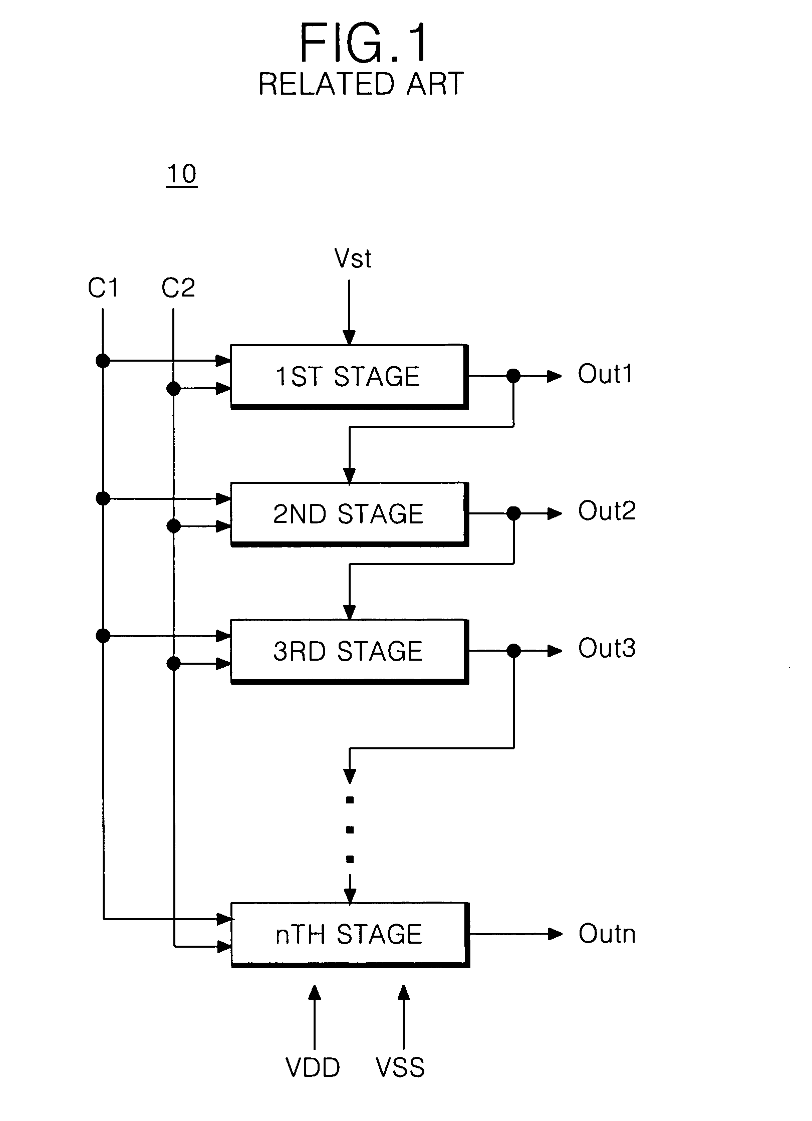
Shift register

Active Publication Date: 2006-07-06
LG DISPLAY CO LTD
View PDF3 Cites 94 Cited by
  • Summary
  • Abstract
  • Description
  • Claims
  • Application Information

AI Technical Summary

Benefits of technology

[0012] In another embodiment, a shift register includes first and second AC voltage supply lines and first and second DC voltage supply lines. The first and second AC voltage supply lines supply first and second AC voltages having opposite polarities in first and second frames. The first and second DC voltage supply lines supply first and second DC voltages, respectively. The shift register further includes at least two clock signal supply lines, a pull-up TFT, and first and second pull-down TFTs. The two clock signal supply lines supply at least two clock signals having different phases. The pull-up TFT is controlled in response to the state of a first node to supply any one of the clock

Problems solved by technology

During this time, the pull-down TFT Tpd may experience malfunc

Method used


Image

  • Shift register
  • Shift register
  • Shift register

Examples


first embodiment

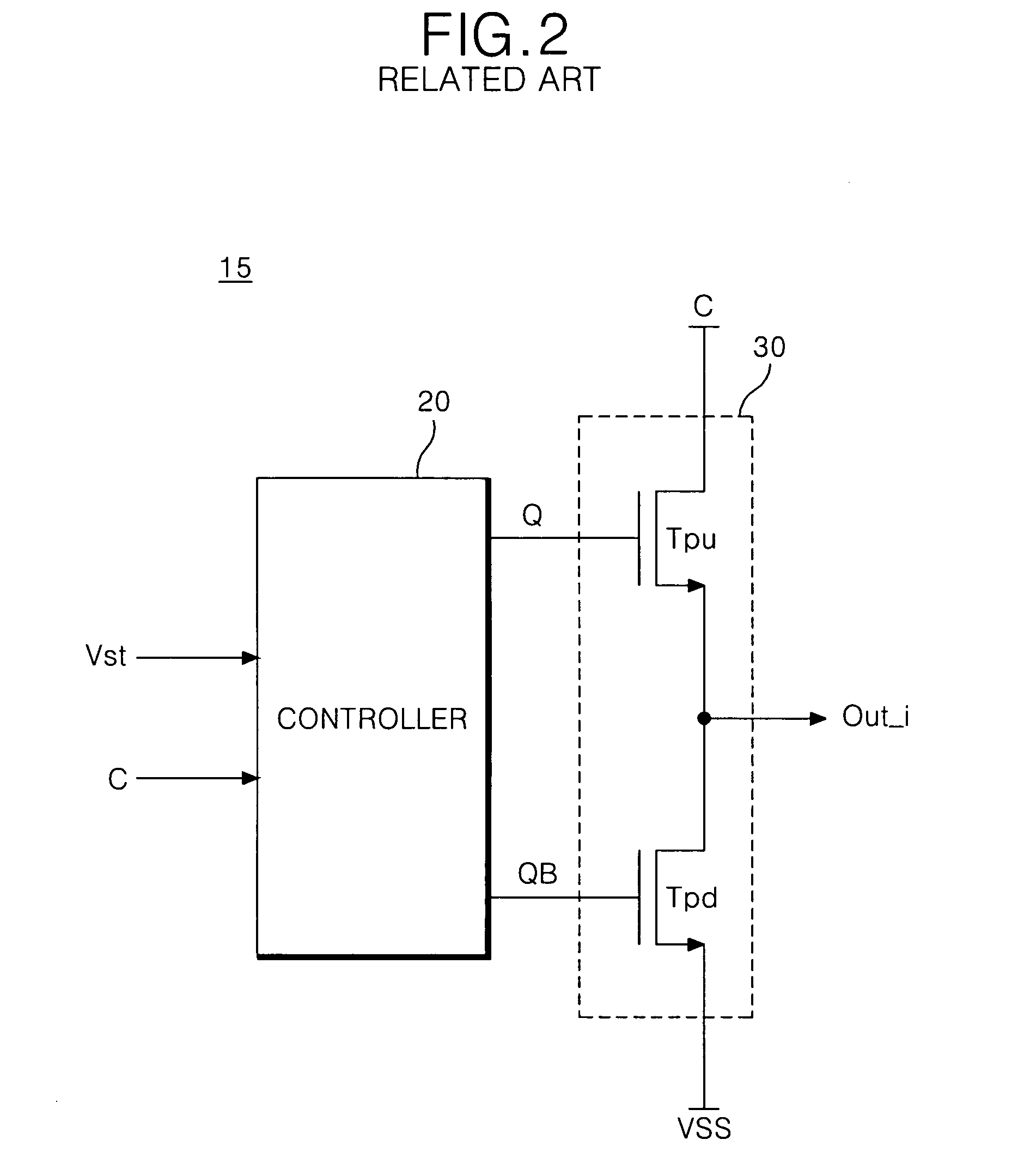
[0022]FIG. 3 illustrates a circuit diagram of one of a plurality of stages connected in cascade a shift register and FIG. 4 illustrates a driving waveform diagram for use with the stage shown in FIG. 3. The stage 100 of the shift register shown in FIG. 3 includes a first controller 35, a second controller 40 and an output buffer 50. The first controller 35 and the second controller 40 may control the output buffer 50 to output different output signals. For example, the first controller 35 and the second controller 40 may activate or deactivate thin film transistors (TFTs) of the output buffer 50. The first controller 35 and the second controller 40 may include TFTs that are activated or deactivated in response to various control signals.

[0023] The output buffer 50 includes a pull-up TFT T6 for outputting a first clock signal C1 to an output line in response to the state of a Q node. The output buffer 50 also includes odd and even pull-down TFTs T7_O, T7_E for outputting a low-level...

second embodiment

[0040]FIG. 5 illustrates a circuit diagram of one of stages connected in cascade in a shift register according to a The stage 500 includes the same components as the stage 100 shown in FIG. 3 and further includes an even TFT T5C_E and an odd TFT T5C_O. The even TFT T5C_E discharges the QB_E node by the first AC voltage VDD_O and the odd TFT T5C_O discharges the QB_O node by the second AC voltage VDD_E.

[0041] The even TFT T5C_E, as shown in FIG. 5, is turned on to supply the low-level voltage VSS to the QB_E node if the first AC voltage VDD_O becomes the high state in the odd frame. The odd TFT T5C_O is turned on to supply the low-level voltage VSS to the QB_O node if the second AC voltage VDD_E becomes the high state in the even frame. In other words, the even TFT T5C_E changes the high-state voltage of the QB_E node to the low-state voltage by applying the low state voltage in the odd frame. The odd TFT T5C_O changes the high-state voltage of the QB_O node to the low-state voltage...

third embodiment

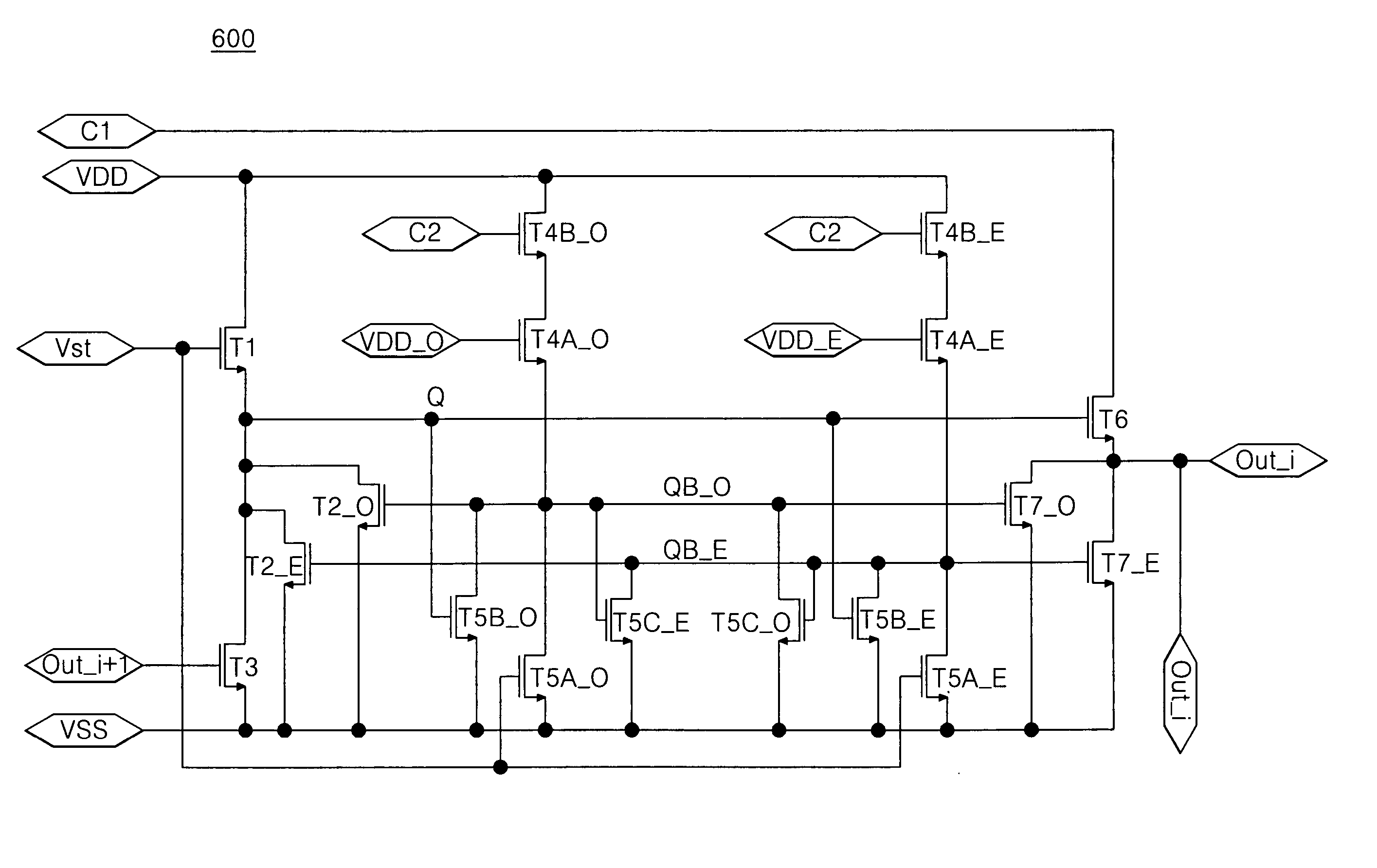
[0042]FIG. 6 illustrates a circuit diagram of one of stages 600 in a shift register according to a Unlike the stage 500 of FIG. 5, the even TFT T5C_E is controlled by the QB_O node and the odd TFT T5C_O is controlled by the QB_E node in FIG. 6. Referring to FIG. 4, the even TFT T5C_E shown in FIG. 6 is turned on by the QB_O node which becomes the high state after a high output voltage Out_i is supplied in the odd frame. The QB_E node remains the low-level voltage VSS. The odd TFT T5C_O is turned on to keep the QB_O node at the low-level voltage VSS if the QB_E node become the high state in the even frame.

[0043] As described above, the shift register may drive the dual pull-down TFT T7_O, T7_E alternately in the odd frame and the even frame. As a result, the gate bias stress may be prevented. Also, the shift register drives the TFTs T4A_O, T4B_O charging the QB_O node and the TFTs T4A_E, T4B_E charging the QB_E node alternately in the odd frame and the even frame. It is possible to ...


PUM


Abstract

A shift register for use with a liquid crystal display device includes a plurality of stages. A stage of the shift register includes a first controller, a second controller and an output buffer. The first controller charges and discharges a first node. The second controller charges and discharges a second node and a third node. The output buffer outputs a first output signal in response to the state of the first node and a second output signal in response to the state of the second and third nodes. The shift register may be adaptive to avoid a malfunction caused by a gate bias stress.

Description

[0001] This application claims the benefit of the Korean Patent Application No. P2004-118606 filed on Dec. 31, 2004, which is hereby incorporated by reference by its entirety. BACKGROUND [0002] 1. Technical Field [0003] The present invention relates to a drive circuit of a liquid crystal display device, and more particularly to a drive circuit having a shift register using an amorphous silicon (a-Si) thin film transistor. [0004] 2. Related Art [0005] A liquid crystal display (LCD) is a display device for use with a television or a computer. The LCD controls light transmittance of a liquid crystal using an electric field to display a picture. To this end, the LCD includes a liquid crystal display panel having liquid crystal cells arranged in a matrix type and a drive circuit for driving the liquid crystal display panel. [0006] The liquid crystal display panel includes a liquid crystal cell formed at each area which is defined by intersecting gate lines and data lines. A thin film tra...

Claims


Application Information

Patent Timeline
IPC IPC(8): G09G3/36
CPCG09G3/3677G09G3/3688G11C19/00G11C19/28G09G3/36H03K23/44
Inventor CHO, NAM WOOKYOON, SOO YOUNGCHUN, MIN DOO
Owner LG DISPLAY CO LTD
Why Eureka
Try Eureka