Semiconductor integrated circuit device and wireless communication system

a technology of integrated circuit devices and semiconductors, applied in the field can solve the problems of large parasitic capacitance of amplifiers, large delay of signals outputted from amplifiers, etc., and achieve the effects of improving the reliability of semiconductor integrated circuit devices, low power consumption, and low power consumption

Inactive Publication Date: 2006-07-06
RENESAS TECH CORP
View PDF1 Cites 8 Cited by
  • Summary
  • Abstract
  • Description
  • Claims
  • Application Information

AI Technical Summary

Benefits of technology

[0009] The regulators increase driving capability by using large-sized transistors of amplifiers to supply a sufficient power supply voltage when the semiconductor integrated circuit device for RF processing is operating normally. As a result, the parasitic capacitance of the amplifiers becomes large.
[0020] (1) Regardless of a considerable change in output currents, a phase margin can be ensured between output of a differential voltage comparator and an output signal of a regulator. As a result, the regulator can be prevented from oscillating abnormally, so that stable power supply voltages can be supplied.
[0021] (2) The semiconductor integrated circuit device allows power supply units to consume a small amount of power in idle mode.
[0022] (3) For the reasons described in (1) and (2) above, low power consumption can be achieved with an improvement in the reliability of the semiconductor integrated circuit device.
[0023] (4) Furthermore, by using the semiconductor integrated circuit to form a wireless communication system, low power consumption can be achieved with an improvement in the performance of the wireless communication system.

Problems solved by technology

As a result, the parasitic capacitance of the amplifiers becomes large.
When a small current consumed by the temperature sensor flows through a final-stage amplifier in the regulators, a delay of a signal outputted from the amplifier becomes large because of the parasitic capacitance.

Method used


Image

  • Semiconductor integrated circuit device and wireless communication system
  • Semiconductor integrated circuit device and wireless communication system
  • Semiconductor integrated circuit device and wireless communication system

Examples


Embodiment Construction

[0030] Hereinafter, embodiments of the present invention will be described with reference to the accompanying drawings. In all drawings for describing the embodiments, in principle, identical members are identified by identical reference numbers and duplicate descriptions of them are omitted.

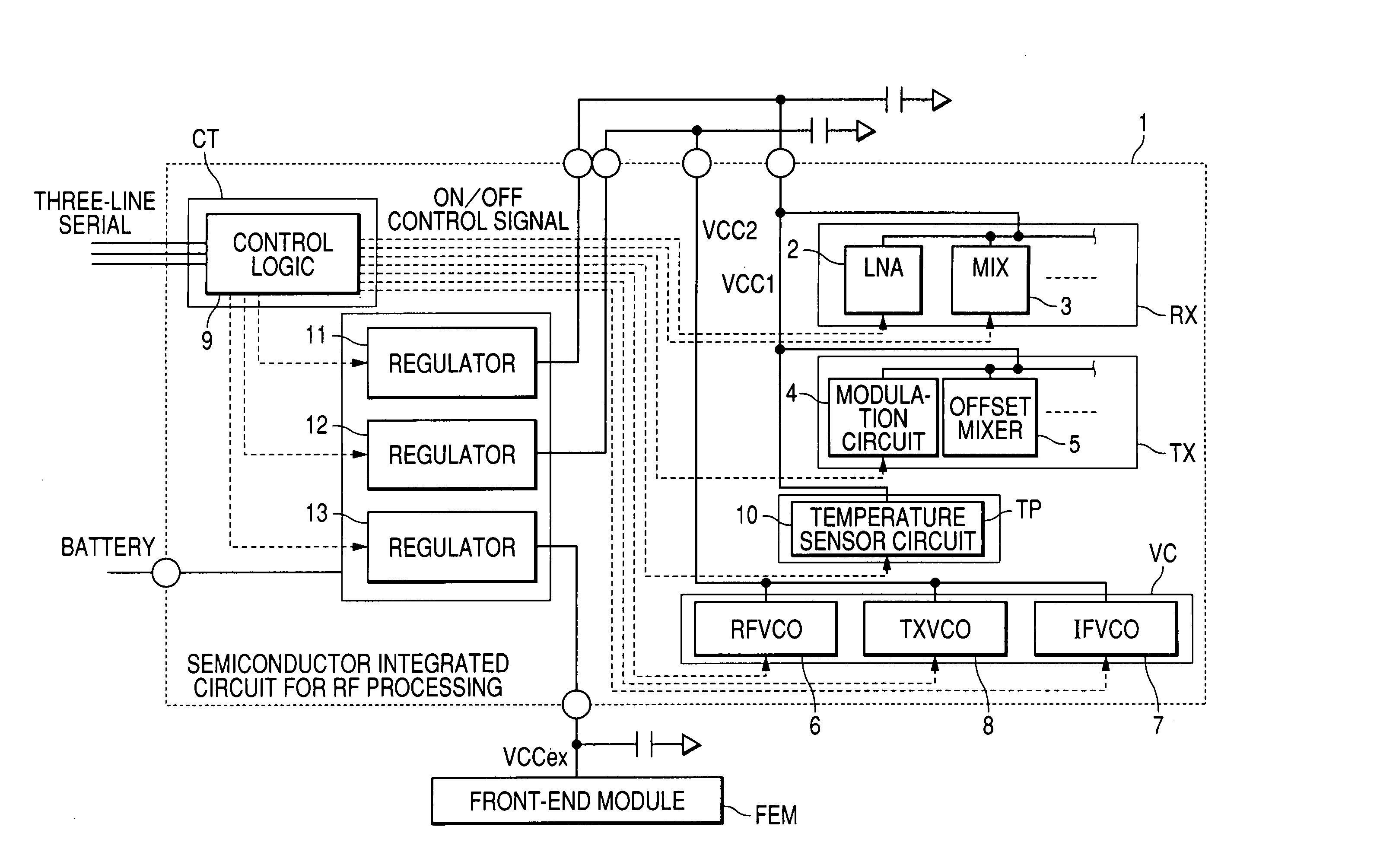
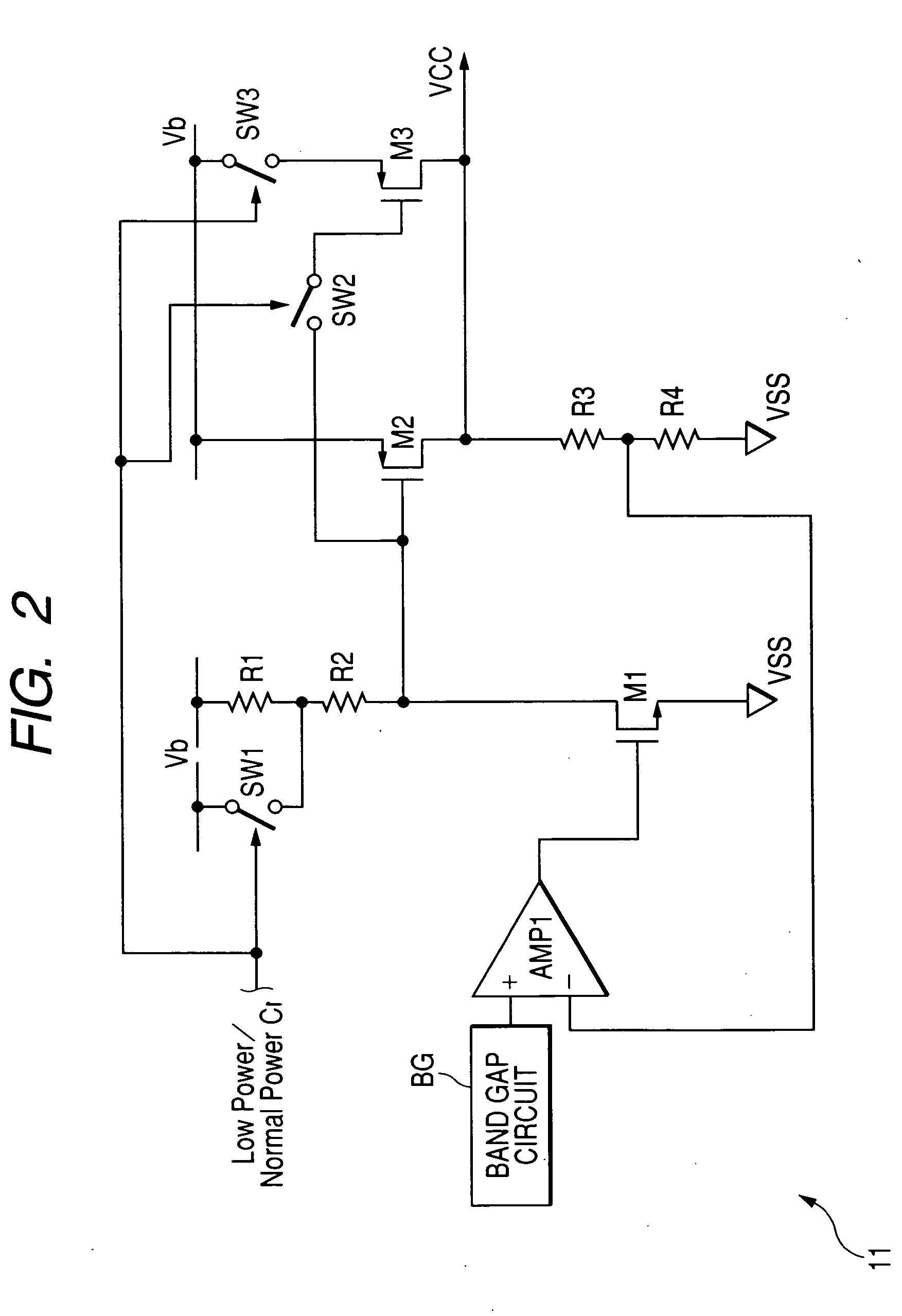
[0031]FIG. 1 is a block diagram of a semiconductor integrated circuit device for RF processing according to one embodiment of the present invention. FIG. 2 is a circuit diagram showing an example of a regulator provided in the semiconductor integrated circuit device for RF processing of FIG. 1. FIG. 3 is a circuit diagram showing another examples of a regulator provided in the semiconductor integrated circuit device for RF processing of FIG. 1. FIG. 4 is a drawing for describing the operation of the regulator in FIG. 2. FIG. 5 is a drawing showing an example of an open loop gain characteristic in the regulator of FIG. 2. FIG. 6 is a drawing for describing the operation of the regulator in FIG. ...


PUM


Abstract

The present invention supplies a stable power supply voltage from small output currents to large output currents, regardless of operation states of a semiconductor integrated circuit device. When an output current of the regulator is small (idle mode), all switches go off. Thereby, power is supplied to a transistor via resistors, a load of a transistor becomes large, and current consumption of the regulator can be reduced. Since a transistor goes off, parasitic capacitance can be reduced, and a sufficient phase margin can be ensured between output of a differential voltage comparator and an output signal of the regulator. In normal operation, all the switches go on, load resistance is reduced to reduce noise, and driving capability is improved to supply stable power supply voltages.

Description

CROSS-REFERENCE TO RELATED APPLICATION [0001] The present application claims priority from Japanese patent application No. 2005-000585 filed on Jan. 5, 2005, the content of which is hereby incorporated by reference into this application. BACKGROUND OF THE INVENTION [0002] The present invention relates to technology for supplying a power supply voltage in a semiconductor integrated circuit device, and more particularly to technology useful for stable supply of an internal power supply voltage in a semiconductor integrated circuit device for radio frequency processing. [0003] In recent years, cellular phones have come into wide use, and have been demanded to have various functions. In such cellular phones, generally, two semiconductor integrated circuit devices, one for RF (radio frequency) processing and the other for baseband processing, are used. [0004] A semiconductor integrated circuit device for RF processing converts a received signal into a baseband signal as a so-called I or ...

Claims


Application Information

Patent Timeline
Patent Type & Authority Applications(United States)
IPC IPC(8): H04B1/00
CPCH04W52/028Y02D30/70
Inventor HARASAWA, YOSHIAKIKASAHARA, MASUMI
Owner RENESAS TECH CORP
Why Eureka
Try Eureka